

METHOD FOR FORMING CONDUCTIVE PATTERN BY DIRECT RADIATION OF ELECTROMAGNETIC WAVE, AND RESIN STRUCTURE HAVING CONDUCTIVE PATTERN THEREON (As Amended)
a technology of electromagnetic wave and conductive pattern, which is applied in the direction of conductive layers on insulating supports, film/foil adhesives, nuclear engineering, etc., can solve the problems of increasing the total manufacturing cost, increasing and deteriorating physical properties, so as to reduce the manufacturing cost of the process the effect of reducing the cost of forming conductive patterns
- Summary
- Abstract
- Description
- Claims
- Application Information
AI Technical Summary
Benefits of technology
Problems solved by technology
Method used
Image

Examples
example 1
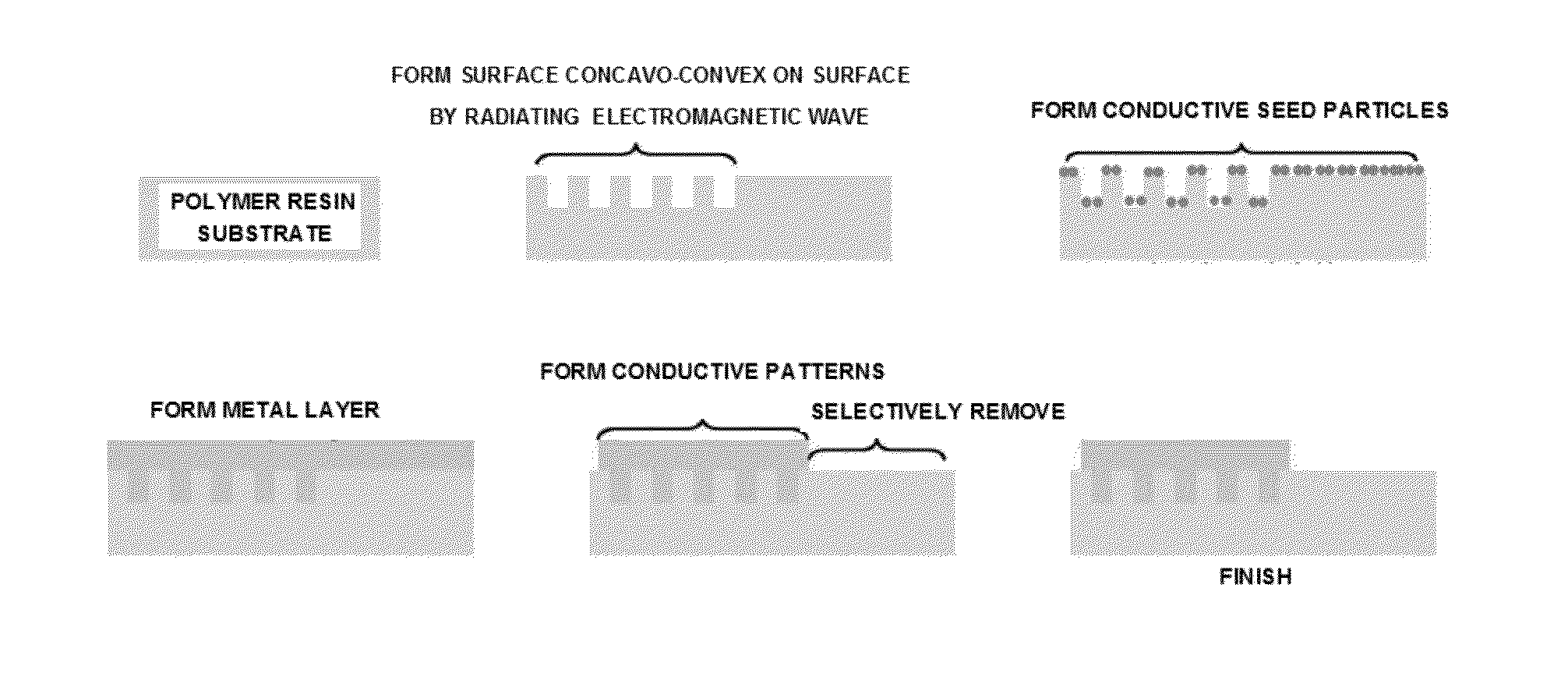
Formation of Conductive Patterns by Laser Direct Radiation
[0080]A polycarbonate resin substrate containing an UV stabilizer, a thermal stabilizer, and an impact reinforcing agent having a total amount of less than 2 wt %, and containing 5 wt % of titanium dioxide (TiO2) was prepared. Here, it could be confirmed that the polycarbonate resin substrate to which titanium dioxide was not added had brightness L* value of 80 to 82; meanwhile, the resin substrate to which titanium dioxide was added had brightness L* value of 95 to 97, which has significantly bright white color, wherein the brightness L* value was measured based on CIE L*a*b* tintometer using colorimeter.
[0081]Laser having a wavelength of 1064 nm was radiated once onto a predetermined region of the polycarbonate resin substrate under radiation condition (average power: 16 W) having an power ratio of 60%. Here, the interval between central parts of the laser radiation trace of the polycarbonate resin substrate was controlled ...
example 2
Formation of Conductive Patterns by Laser Direct Radiation
[0088]Conductive patterns of Example 2 were formed by the same method as Example 1 except that the radiation condition of the laser was changed into the radiation condition (average power: 20 W) having an power ratio of 75%.
[0089]In Example 2, after radiating laser, the center line arithmetic average roughness of the absolute values (Ra) of the region radiated by laser and the region which is not radiated by laser were measured by the same method as Example 1, and the region radiated by laser had Ra of about 3820 nm and the region which is not radiated by laser had Ra of about 152 nm, respectively.
[0090]In addition, after the metal layer and the conductive patterns were formed in Example 2, a cross-cut test was conducted by the same method as Example 1 in the region having the metal layer and the conductive patterns formed thereon. As a result of the adhesion test, it could be confirmed that the delamination area of the targe...
reference example 1
Formation of Conductive Patterns by Laser Direct Radiation (Using Specific Inorganic Additive)
[0097]A polycarbonate resin substrate containing an UV stabilizer, a thermal stabilizer, and an impact reinforcing agent having a total amount of less than 2 wt %, and containing 3 wt % of inorganic additive (Cu2(OH)PO4) (ivory color) was prepared. Here, it could be confirmed that the polycarbonate resin substrate to which titanium dioxide was not added had brightness L* value of 80 to 82; meanwhile, the resin substrate to which the inorganic additive was added had brightness L* value of 89 to 91, which had dark color as compared to Example 1, wherein the brightness L* value was measured based on CIE L*a*b* tintometer using colorimeter, and thus, additional white pigment, and the like, are required in implementing final white color.
[0098]Laser having a wavelength of 1064 nm was radiated once onto a predetermined region of the polycarbonate resin substrate under radiation condition (average ...
PUM
| Property | Measurement | Unit |
|---|---|---|
| particle diameter | aaaaa | aaaaa |
| adhesion | aaaaa | aaaaa |
| width | aaaaa | aaaaa |
Abstract
Description
Claims
Application Information