Method to make buried, highly conductive p-type iii-nitride layers

a technology of iii-nitride and p-type layers, which is applied in the direction of diodes, semiconductor devices, electrical apparatus, etc., can solve the problems of limiting device performance and reducing the operating speed of transistors or diodes, and achieve the effect of reducing the resistance of p-type layers

Active Publication Date: 2016-07-07
YALE UNIV
View PDF7 Cites 27 Cited by
  • Summary
  • Abstract
  • Description
  • Claims
  • Application Information

AI Technical Summary

Benefits of technology

[0008]Methods and structures relating to the formation of highly-conductive, p-type layers in III-nitride integrated devices are described. One or more conductive, porous layers may be formed adjacent to a p-type layer. The porous layer can provide a pathway for hydrogen from the p-type layer to diffuse out of the device during an annealing step. By allowing hydrogen to escape from a p-type layer, a larger number of acceptor dopants may be activated, thereby reducing the resistance of the p-type layer. The porous layers may remain highly conductive and be incorporated as active layers into diodes, transistors, light-emitting diodes, and laser diodes, among other devices.

Problems solved by technology

A high resistivity of a p-type layer may limit device performance.
For example, a highly resistive p-type layer may reduce an operating speed of a transistor or diode.

Method used


Image

  • Method to make buried, highly conductive p-type iii-nitride layers
  • Method to make buried, highly conductive p-type iii-nitride layers
  • Method to make buried, highly conductive p-type iii-nitride layers

Examples


Embodiment Construction

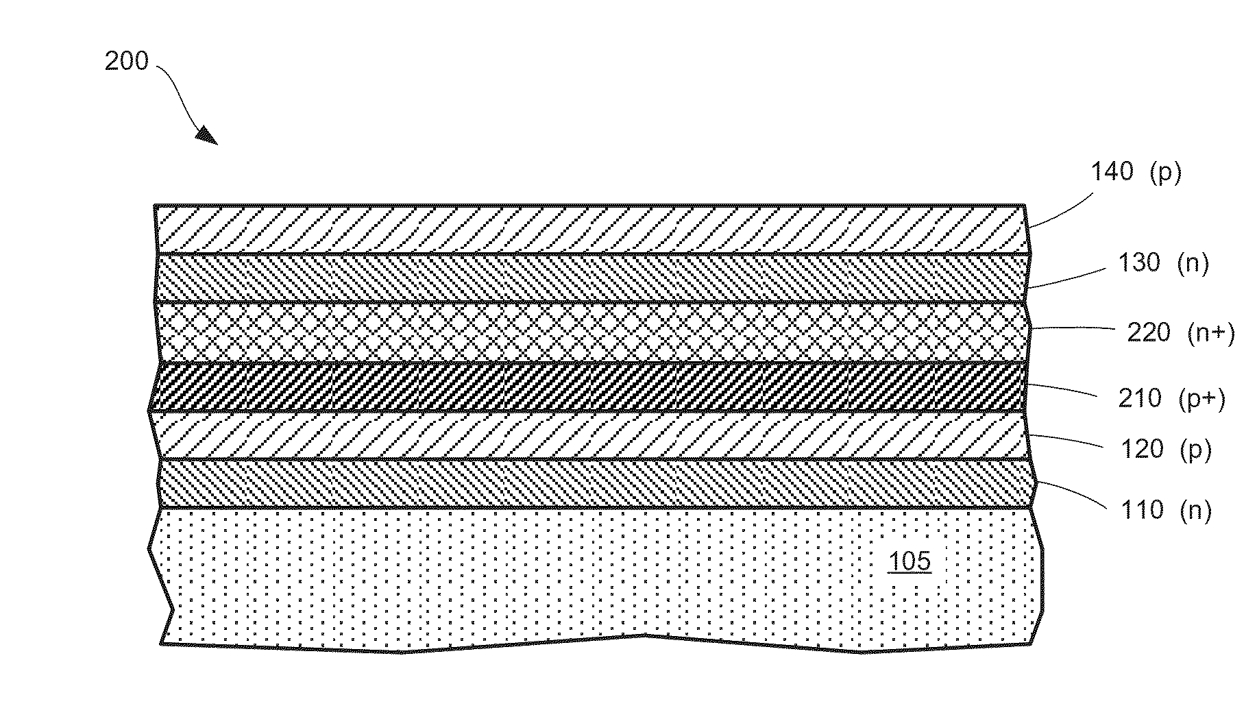
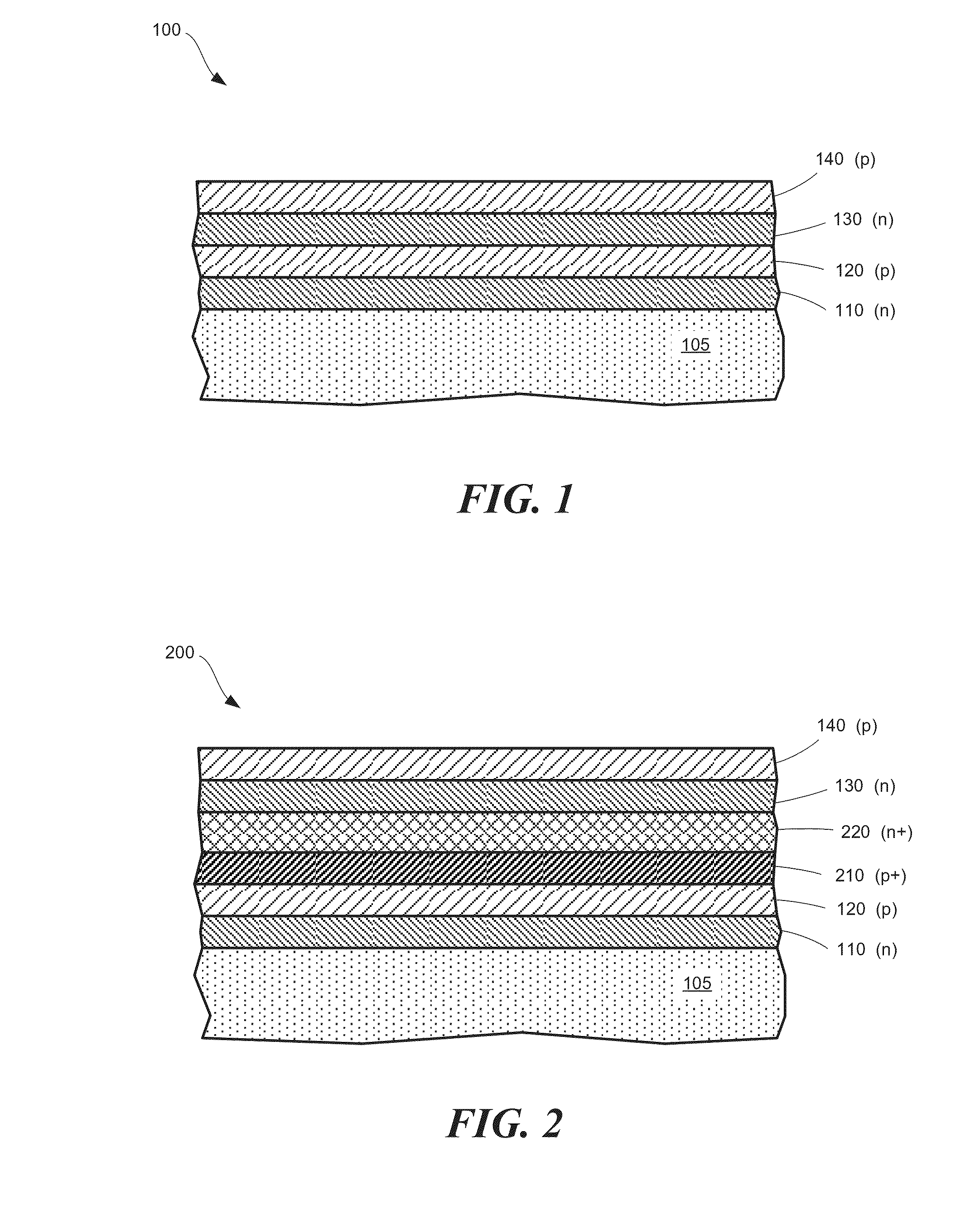
[0029]The inventors have recognized and appreciated that, in some cases, conventional, p-type, III-nitride layers (such as Mg-doped AlInGaN) that are formed using MOCVD or HYPE still suffer from a low dopant activation percentage and exhibit reduced p-type conductivity. Low dopant activation is more noticeable for integrated devices in which an acceptor-doped layer is embedded underneath one or several other layers in an epitaxy structure, such as a multilayer stack depicted in FIG. 1. The structure 100 in FIG. 1 includes cascaded pn junctions formed on a substrate 105, and may be used for a III-nitride tandem solar cell, for example. Even though a thermal annealing step may be used during the fabrication process, the inventors have recognized and appreciated that hydrogen cannot easily diffuse from a buried p-type layer 120 through the upper layers 130, 140 and be released into an ambient.

[0030]Although hydrogen could diffuse laterally along a p-type layer 120, the inventors have r...


PUM

PropertyMeasurementUnit
thicknessaaaaaaaaaa
pore diametersaaaaaaaaaa

Abstract

A conductive, porous gallium-nitride layer can be formed as an active layer in a multilayer structure adjacent to one or more p-type III-nitride layers, which may be buried in a multilayer stack of an integrated device. During an annealing process, dopant-bound atomic species in the p-type layers that might otherwise neutralize the dopants may dissociate and out-diffuse from the device through the porous layer. The release and removal of the neutralizing species may reduce layer resistance and improve device performance.

Description

CROSS REFERENCE TO RELATED APPLICATION[0001]This application claims the benefit of U.S. Provisional Application No. 62 / 086,020, filed Dec. 1, 2014, titled “A Method to Make Buried, Highly Conductive P-Type III-Nitride Layers,” which is hereby incorporated by reference in its entirety.BACKGROUND[0002]1. Technical Field[0003]The technology relates to III-nitride integrated devices that include p-type layers having neutralizing atomic species bound to acceptors.[0004]2. Discussion of the Related Art[0005]Gallium-nitride crystals were produced at the end of the 1960s by growing GaN on a substrate using a hydride vapor phase epitaxy (HVPE) technique. In the 1970s, new crystal-growth techniques were developed for growing semiconductors on substrates. These new techniques included molecular beam epitaxy (MBE) and metalorganic vapor phase epitaxy (MOVPE) which is also known as metalorganic chemical vapor deposition (MOCVD). For each of these techniques, an epitaxial layer may be doped with ...

Claims


Application Information

Patent Timeline
Patent Type & Authority Applications(United States)
IPC IPC(8): H01L29/20H01L33/32H01L31/0304H01L21/308H01L29/207H01L21/02H01L21/324H01L21/306H01L29/78H01L29/861
CPCH01L29/2003H01L29/78H01L33/32H01L31/03044H01L21/3081H01L29/207H01L21/0254H01L21/3245H01L21/30612H01L29/861H01L21/306H01L33/16H01L33/40H01L2933/0016H01L29/88H01L29/15H01L31/0725H01L31/0735H01L31/1856Y02E10/544H01L31/035236H01L31/036
Inventor HAN, JUNGLI, YUFENGZHANG, CHENGPARK, SUNG HYUN
Owner YALE UNIV
Why Eureka
Try Eureka