Silicon carbide substrate, silicon carbide semiconductor device, and method for manufacturing silicon carbide substrate

a silicon carbide substrate and semiconductor technology, applied in the direction of semiconductor devices, electrical equipment, basic electric elements, etc., can solve the problems of high resistance and deterioration of dielectric breakdown resistance of gate insulating films provided on silicon carbide epitaxial layers, and achieve the effect of suppressing the dielectric breakdown of gate insulating films

Inactive Publication Date: 2016-07-07
SUMITOMO ELECTRIC IND LTD
View PDF6 Cites 14 Cited by
  • Summary
  • Abstract
  • Description
  • Claims
  • Application Information

AI Technical Summary

Benefits of technology

[0008]One embodiment of the present invention has an object to provide a silicon carbide substrate, a silicon carbide semiconductor device, and a method for manufacturing the silicon carbide substrate, by each of which carrier lifetime can be improved and dielectric breakdown of a gate insulating film can be suppressed.

Problems solved by technology

In particular, in a bipolar semiconductor device, short carrier lifetime does not lead to sufficient conductivity modulation, thus resulting in high on resistance.
However, in the case of a silicon carbide semiconductor device employing a thick silicon carbide epitaxial layer having a thickness of, for example, about not less than 50 μm and having Z1 / 2 centers reduced by thermally oxidizing the surface of the silicon carbide epitaxial layer and then performing annealing, the dielectric breakdown resistance of a gate insulating film provided on the silicon carbide epitaxial layer may be deteriorated.

Method used


Image

  • Silicon carbide substrate, silicon carbide semiconductor device, and method for manufacturing silicon carbide substrate
  • Silicon carbide substrate, silicon carbide semiconductor device, and method for manufacturing silicon carbide substrate
  • Silicon carbide substrate, silicon carbide semiconductor device, and method for manufacturing silicon carbide substrate

Examples


first embodiment

Silicon Carbide Substrate

[0040]First, the following describes a configuration of a silicon carbide substrate 10 according to a first embodiment of the present invention.

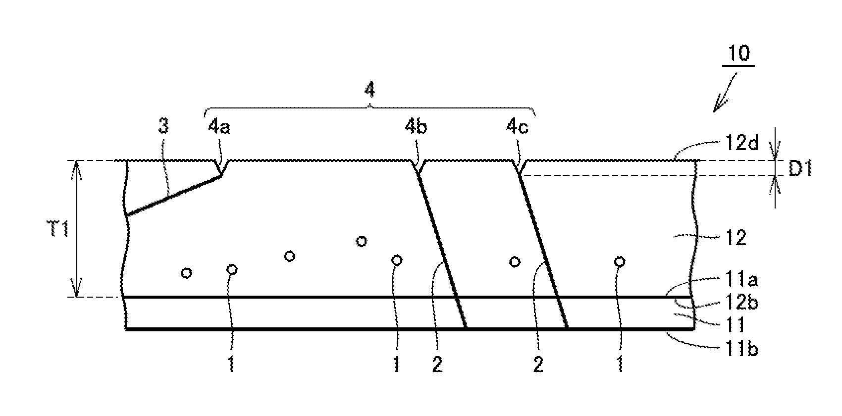
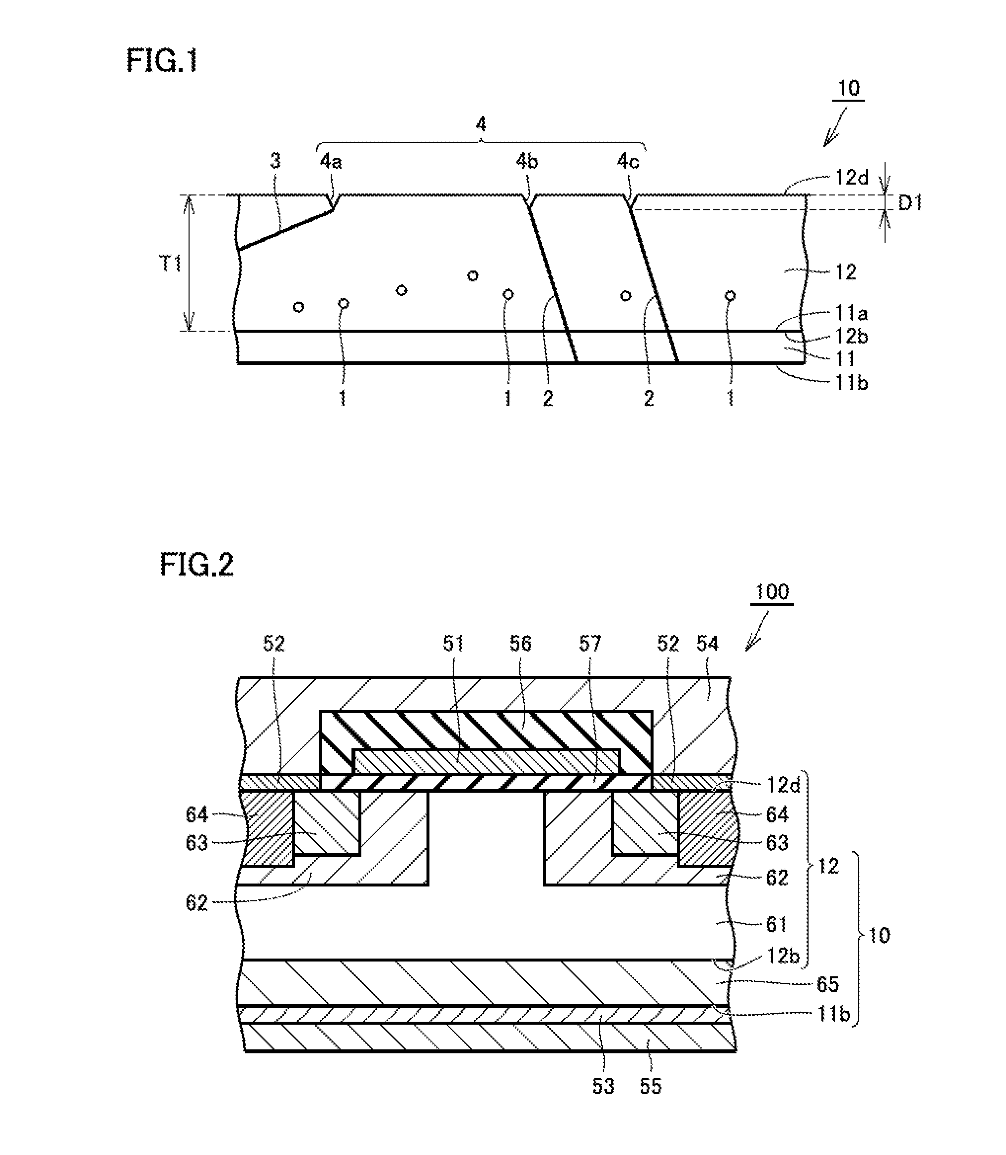
[0041]As shown in FIG. 1, a silicon carbide substrate 10 according to the present embodiment mainly includes a silicon carbide single crystal substrate 11 and a silicon carbide epitaxial layer 12. Silicon carbide single crystal substrate 11 is made of hexagonal silicon carbide having polytype 4H, for example. Silicon carbide epitaxial layer 12 is provided on silicon carbide single crystal substrate 11. Silicon carbide epitaxial layer 12 has a first main surface 12b in contact with silicon carbide single crystal substrate 11 and a second main surface 12d opposite to first main surface 12b. Silicon carbide epitaxial layer 12 has a thickness T1 of not less than 50 μm in a direction perpendicular to second main surface 12d. Preferably, thickness T1 of silicon carbide epitaxial layer 12 is not less than 100 μm, more prefe...

second embodiment

Silicon Carbide Semiconductor Device

[0050]Next, the following describes a configuration of an IGBT (Insulated Gate Bipolar Transistor) as a silicon carbide semiconductor device 100 according to a second embodiment of the present invention.

[0051]As shown in FIG. 2, IGBT 100 according to the present embodiment is a bipolar semiconductor device mainly including silicon carbide epitaxial layer 12, a gate insulating film 57, a gate electrode 51, an interlayer insulating film 56, an emitter electrode 52, a collector electrode 53, an upper interconnection 54, and a lower interconnection 55. Silicon carbide substrate 10 mainly includes silicon carbide epitaxial layer 12 and a collector region 65.

[0052]Silicon carbide epitaxial layer 12 has first main surface 12b and second main surface 12d opposite to first main surface 12b. There are pits 4 in second main surface 12d of silicon carbide epitaxial layer 12, and each of pits 4 originates from threading dislocations 2 or basal plane dislocatio...

third embodiment

Method for Manufacturing Silicon Carbide Substrate

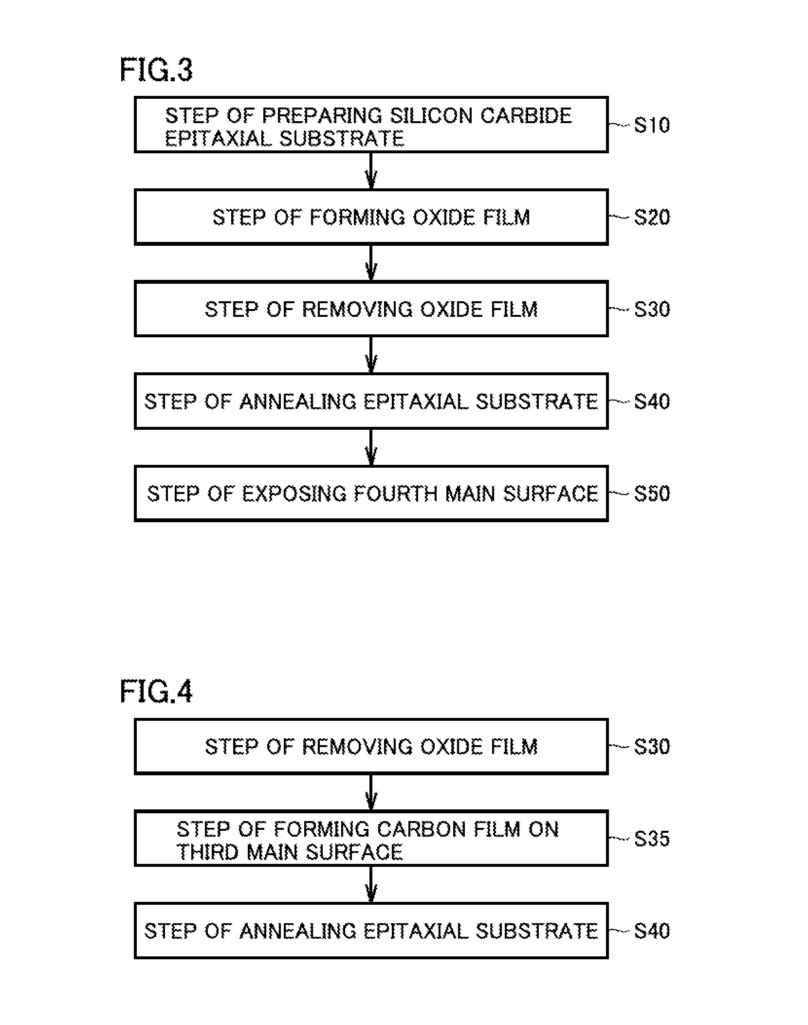
[0060]Next, the following describes a method for manufacturing silicon carbide substrate 10 according to a third embodiment of the present invention.

[0061]First, a step (S10: FIG. 3) of preparing a silicon carbide epitaxial substrate is performed. For example, silicon carbide single crystal substrate 11 is prepared by slicing a silicon carbide single crystal ingot. The polytype of the silicon carbide is 4H, for example. Silicon carbide single crystal substrate 11 has a front surface 11a and a backside surface 11b, for example. Front surface 11a of silicon carbide single crystal substrate 11 corresponds to a {0001} plane or a plane angled off relative to the {0001} plane, for example. Front surface 11a has an off angle of for example, not less than 1° and not more than 8°, preferably, not less than 2° and not more than 7°, and more preferably, not less than 3° and not more than 5°. The off direction is a direction, for example. Silic...


PUM

PropertyMeasurementUnit
thicknessaaaaaaaaaa
depthaaaaaaaaaa
breakdown voltageaaaaaaaaaa

Abstract

A silicon carbide substrate has a silicon carbide epitaxial layer. The silicon carbide epitaxial layer has a first main surface and a second main surface opposite to the first main surface. The silicon carbide epitaxial layer has a thickness of not less than 50 μm in a direction perpendicular to the second main surface. Z1/2 centers are in the silicon carbide epitaxial layer at a density of not more than 1×1012 cm−3. A pit has a maximum depth of not more than 5 nm, the pit originating from a threading dislocation or a basal plane dislocation and having an opening at the second main surface.

Description

BACKGROUND OF THE INVENTION[0001]1. Field of the Invention[0002]The present invention relates to a silicon carbide substrate, a silicon carbide semiconductor device, and a method for manufacturing the silicon carbide substrate.[0003]2. Description of the Background Art[0004]Silicon carbide has high dielectric breakdown electric field strength and is therefore drawing attention as a material for next-generation power semiconductor devices to replace silicon.SUMMARY OF THE INVENTION[0005]In order to realize a silicon carbide power semiconductor device having a high breakdown voltage of, for example, not less than 5 kV, a thick silicon carbide epitaxial layer having a thickness of about not less than 50 μm is needed. Point defects, which are called Z1 / 2 centers and originate from carbon vacancy, are in the silicon carbide epitaxial layer. Each of the Z1 / 2 centers has an energy level of Ec (the lowest energy in the conduction band)−0.65 eV. The Z1 / 2 centers are a so-called lifetime kill...

Claims


Application Information

Patent Timeline
Patent Type & Authority Applications(United States)
IPC IPC(8): H01L29/423H01L21/04H01L21/324H01L29/16H01L29/66
CPCH01L29/42364H01L29/1608H01L29/66068H01L29/42356H01L21/3247H01L21/0475H01L29/66477H01L29/0661H01L29/78H01L21/02008H01L21/324H01L21/02378H01L21/02529H01L21/02587H01L21/0262H01L21/02664H01L21/02236H01L21/302H01L21/30604H01L21/30625H01L29/7395H01L29/868H01L29/872
Inventor HIYOSHI, TORU
Owner SUMITOMO ELECTRIC IND LTD
Why Eureka
Try Eureka