
Nanostructured copper-selenide with high thermoelectric figure-of-merit and process for the preparation thereof

a technology of nanostructured copper and selenide, which is applied in the field of nanostructured copperselenide with high thermoelectric figure of merit and process for the preparation of it, can solve the problems of low thermoelectric device conversion efficiency, limited commercial applications, and high cost of silver and tellurium, and achieves rapid heating rate and cost-effective

Inactive Publication Date: 2016-08-04
COUNCIL OF SCI & IND RES
View PDF2 Cites 5 Cited by
  • Summary
  • Abstract
  • Description
  • Claims
  • Application Information

AI Technical Summary

Benefits of technology

The present invention provides a cost-effective and non-toxic thermoelectric material with high thermoelectric figure of merit. This material can be synthesized using a quick process using spark plasma sintering techniques.

Problems solved by technology

Most of the currently available thermoelectric materials have lower figure-of-merit leading to low conversion efficiency of the thermoelectric device and thus these materials have limited commercial applications.
However, LAST alloy contains Lead which is very toxic, Silver and Tellurium which are quite expensive.
472-478) have prepared nanostructured Cu2Se by ball milling, but they have sintered these nanopowders by hot pressing route, which is known to result in grain growth.

Method used


Image

  • Nanostructured copper-selenide with high thermoelectric figure-of-merit and process for the preparation thereof
  • Nanostructured copper-selenide with high thermoelectric figure-of-merit and process for the preparation thereof
  • Nanostructured copper-selenide with high thermoelectric figure-of-merit and process for the preparation thereof

Examples


example 1

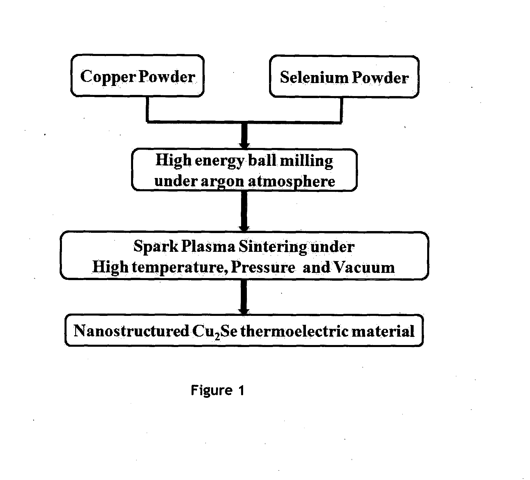
[0049]6.168 gm of Cu powder (99.99%, Alfa Aesar) and 3.832 gm of Se powders (99.99%, Alfa Aesar) were mixed in and milled in a high energy planetary ball mill with 0.2 gm of Stearic acid powder in 250 ml grinding jars made of hardened stainless steel and using 10 mm diameter grinding balls also made of ball hardened stainless in ball to powder weight ratio of 15:1 for 50 hours at a speed of 400 rpm, in an inert atmosphere of argon gas, resulting in the nanostructured powders of Cu and Se.

[0050]After ball milling the powders of Cu and Se were handled only in a glove box under high purity argon to avoid any oxidation and atmospheric contamination. These high energy ball milled nanostructured Cu and Se powders were compacted in 12.7 mm inner diameter high strength graphite on a hydraulic press at a pressure of 0.3 MPa in a form of a pellet.

[0051]This compacted pellet of nanostructured Cu and Se nanopowders was then consolidated using spark plasma sintering process at a pressure of 60 M...

example 2

[0052]24.672 gm of Cu powder (99.99%, Alfa Aesar) and 15.328 gm of Se powders (99.99%, Alfa Aesar) were mixed in, and milled in a high energy planetary ball mill with 0.8 gm of Stearic acid powder in 500 ml grinding jars made of hardened stainless steel and using 10 mm diameter grinding balls also made of ball hardened stainless in ball to powder weight ratio of 20:1 for 50 hours at a speed of 400 rpm, in an inert atmosphere of argon gas, resulting in the nanostructured powders of Cu and Se.

[0053]After ball milling the powders of Cu and Se were handled only in a glove box under high purity argon to avoid any oxidation and atmospheric contamination. These high energy ball milled nanostructured Cu and Se powders were compacted in 12.7 mm inner diameter high strength graphite on a hydraulic press at a pressure of 0.5 MPa in a form of a pellet.

[0054]This compacted pellet of nanostructured Cu and Se nanopowders was then consolidated using spark plasma sintering process at a pressure of 6...

example 3

[0055]6.168 gm of Cu powder (99.99%, Alfa Aesar) and 3.832 gm of Se powders (99.99%, Alfa Aesar) were mixed in and milled in a high energy planetary ball mill in 250 ml grinding jars made of hardened stainless steel and using 10 mm diameter grinding balls also made of ball hardened stainless in ball to powder weight ratio of 20:1 for 40 hours at a speed of 400 rpm, in an inert atmosphere of argon gas, resulting in the nanostructured powders of Cu and Se.

[0056]After ball milling the powders of Cu and Se were handled only in a glove box under high purity argon to avoid any oxidation and atmospheric contamination. These high energy ball milled nanostructured Cu and Se powders were compacted in 12.7 mm inner diameter high strength graphite on a hydraulic press at an pressure of 0.3 MPa in a form of a pellet.

[0057]This compacted pellet of nanostructured Cu and Se nanopowders was then consolidated using spark plasma sintering process at a pressure of 60 MPa and temperature of 873 K with a...


PUM


Abstract

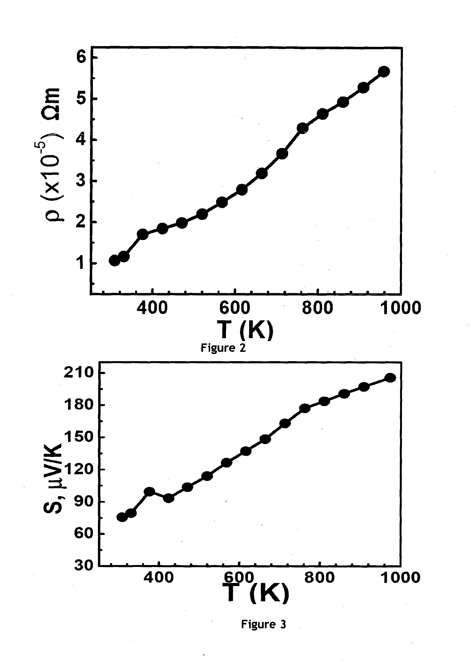
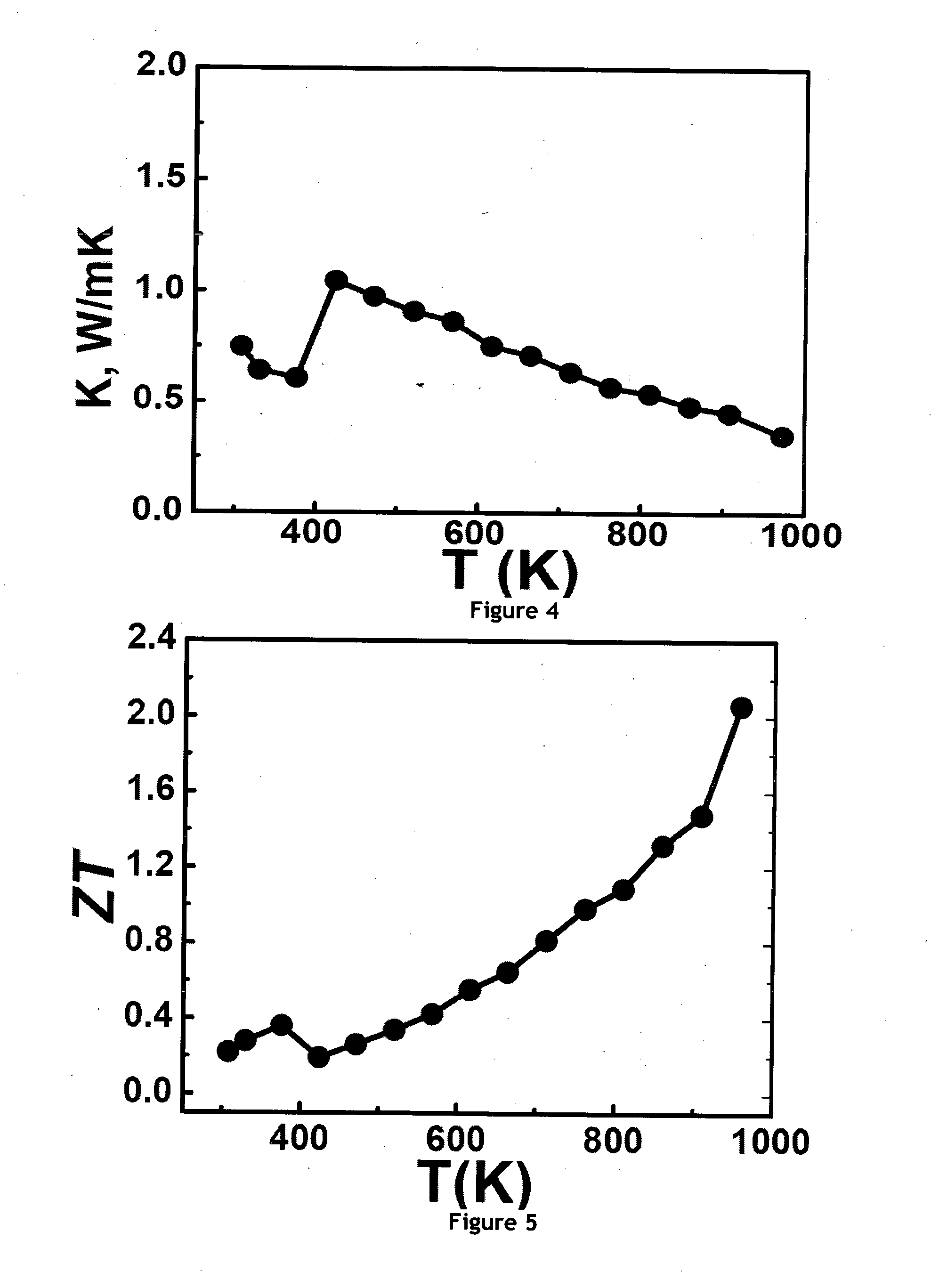
Disclosed is a nanostructured p-type copper-selenide as a cost-effective thermoelectric material with a high thermoelectric figure-of-merit. The nanostructured copper-selenide is a cost-effective p-type thermoelectric material having a high figure-of-merit of 2 at 973 K and is synthesized employing high energy ball milling process followed by reaction sintering under pressure at high heating rates using spark plasma sintering of the resulting nanopowders. The sintered copper-selenide shows a density of 99.9% of theoretical density and retains the nanoscale features introduced during ball milling leading to a thermoelectric figure of merit of 2 at 973 K.

Description

FIELD OF THE INVENTION[0001]The present invention relates to a process for the synthesis of nanostructured p-type copper-selenide as a non-toxic thermoelectric material with a high thermoelectric figure-of-merit. Particularly, the present invention relates to an improved process for the synthesis of nanostructured p-type B-phase copper-selenide (Cu2Se) with high thermoelectric figure-of-merit of 2 at 973 K useful as p-type thermoelectric element in thermoelectric device for generation of electricity.BACKGROUND OF THE INVENTION[0002]Thermoelectric devices convert waste heat into electricity the conversion efficiency of which depends on the thermoelectric material's figure-of-merit. The thermoelectric figure of merit (ZT) is given by, ZT=S2σT / κ, where S is the Seebeck coefficient, σ is the electrical conductivity, κ the thermal conductivity and T is the temperature.[0003]Most of the currently available thermoelectric materials have lower figure-of-merit leading to low conversion effic...

Claims


Application Information

Patent Timeline
IPC IPC(8): H01L35/16C01B19/00
CPCB82Y30/00H01L35/16H01L35/26C01B19/007C01P2006/40C01P2004/03C01P2004/64C01P2002/60C01P2002/74H10N10/857H10N10/852
Inventor GAHTORI, BHASKERBATHULA, SIVAIAHTYAGI, KRITISRIVASTAVA, AVANISH KUMARDHAR, AJAYBUDHANI, RAMESH CHANDRA
Owner COUNCIL OF SCI & IND RES
Learn More