Integrated high side gate driver structure and circuit for driving high side power transistors

a driver structure and driver technology, applied in transistors, electronic switching, pulse techniques, etc., can solve the problem of adding component and assembly costs to the integrated class d audio amplifier in an extent that is unacceptabl

Active Publication Date: 2016-11-17
INFINEON TECH AUSTRIA AG
View PDF1 Cites 17 Cited by
  • Summary
  • Abstract
  • Description
  • Claims
  • Application Information

AI Technical Summary

Benefits of technology

[0007]The semiconductor substrate may comprise a P type or N type epitaxial semiconductor substrate. The present high side gate driver structure comprises a novel type of double junction isolated well structure due to the presence of the first and second well diffusions or well structures where the second well diffusion is arranged inside the first well diffusion. The first well diffusion may comprise P polarity semiconductor material and the second well diffusion N polarity semiconductor material or vice versa depending on the polarity of the semiconductor substrate. The present high side gate driver structure is capable of substantially eliminating the parasitic well capacitance associated with the first well diffusion to the semiconductor substrate at the high side positive supply voltage port of the gate driver. This parasitic well capacitance is moved to the high side negative supply voltage port of the gate driver which may be connected to an output terminal of a power transistor of a class D amplifier or AC motor driver wherein the high side gate driver structure is integrated. Such a power transistor output terminal for example a source terminal or a MOSFET or IGBT inherently possesses a very low output impedance and high current delivery capability such that parasitic charging and discharging current to the parasitic well capacitance is delivered without inducing ripple voltage on the output terminal and output voltage of class D amplifier or motor driver. Hence, the change of electrical connection of the parasitic well capacitance from the high side positive supply voltage port of the gate driver to the high side negative supply voltage port of the gate driver as accomplished by the present high side gate driver structure eliminates the need of the above-discussed traditional external bootstrap capacitors for smoothing the high side DC voltage that must be supplied to the high side positive supply voltage port of the gate driver.
[0028]The floating voltage regulator may comprise a linear regulator with a pass transistor. The pass transistor may comprise a LDNMOS or LDPMOS transistor having drain-source terminals coupled between the positive voltage input of the regulator and the regulated DC voltage output. The gate driver may comprise an integrated high side gate driver structure according to any of the above-described embodiments thereof to exploit the above-mentioned advantages of this structure. The use of a regulated DC voltage for the supply of power to the gate driver means that a stable and accurate gate signal voltage can be applied to a control terminal of an output transistor of class D amplifier or motor driver to harvest the above-mentioned advantages of this feature. The output or power transistor may comprise an LDMOS transistor such as LDNMOS transistor or LDPMOS transistor while the gate driver may comprise exclusively low voltage MOS transistors with the above-mentioned characteristics. The gate driver may comprise any of the above-mentioned transistor drivers.

Problems solved by technology

However, such external capacitor(s) adds component and assembly costs to the integrated class D audio amplifier to an extent that is unacceptable in numerous types of applications such as high-volume consumer audio systems.

Method used


Image

  • Integrated high side gate driver structure and circuit for driving high side power transistors
  • Integrated high side gate driver structure and circuit for driving high side power transistors
  • Integrated high side gate driver structure and circuit for driving high side power transistors

Examples


Embodiment Construction

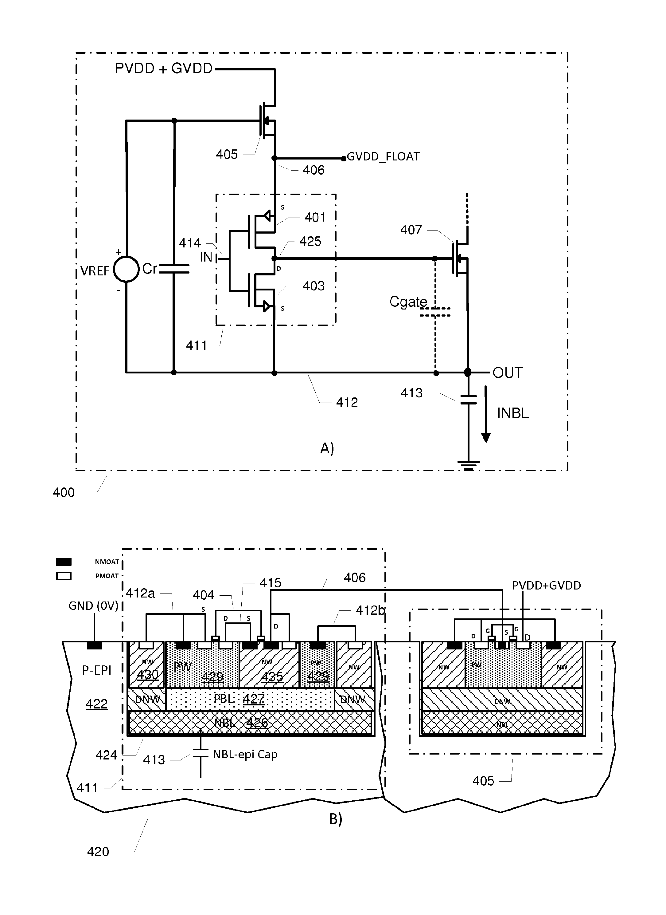
[0037]FIG. 1 is a simplified schematic circuit diagram of a class D amplifier output stage 100. The class D amplifier output stage 100 comprises a prior art integrated high side gate driver structure or circuit, GD, 103. The integrated high side gate driver or circuit 103 has a driver output 104 electrically coupled or connected to a gate terminal of an NMOS power transistor 107 on a high side of the class D output stage. The source terminal of the NMOS power transistor 107 is coupled to a load node or terminal OUT which is connectable to a loudspeaker load for production of sound. The drain terminal of the NMOS power transistor 107 is coupled to a positive DC voltage supply or rail PVDD of the class D output stage. The class D output stage further comprises a low side NMOS power transistor 127 which has a drain terminal coupled to the load terminal OUT such that the loudspeaker load is driven in a push-pull fashion by alternatingly connecting the loudspeaker to the positive DC volt...


PUM


Abstract

The present invention relates to an integrated high side gate driver structure for driving a power transistor. The high side gate driver structure comprises a semiconductor substrate comprising a first polarity semiconductor material in which a first well diffusion comprising a second polarity semiconductor material is formed. A peripheral outer wall of the first well diffusion is abutted to the semiconductor substrate. A second well diffusion, comprising first polarity semiconductor material, is arranged inside the first well diffusion such that an outer peripheral wall of the second well diffusion is abutted to an inner peripheral wall of the first well diffusion. The integrated high side gate driver structure further comprises a gate driver comprising a high side positive supply voltage port, a high side negative supply voltage port, a driver input and a driver output, wherein the gate driver comprises a transistor driver arranged in the second well diffusion such that a control terminal of the transistor driver and an output terminal of the transistor driver is coupled to the driver input and the driver output, respectively; the integrated high side gate driver structure also comprises a first electrical connection between the first well diffusion and the high side negative supply voltage port and a second electrical connection between the second well diffusion and the high side negative supply voltage port.

Description

[0001]The present invention relates to an integrated high side gate driver structure for driving a power transistor. The high side gate driver structure comprises a semiconductor substrate comprising a first polarity semiconductor material in which a first well diffusion comprising a second polarity semiconductor material is formed. A peripheral outer wall of the first well diffusion is abutted to the semiconductor substrate. A second well diffusion, comprising first polarity semiconductor material, is arranged inside the first well diffusion such that an outer peripheral wall of the second well diffusion is abutted to an inner peripheral wall of the first well diffusion. The integrated high side gate driver structure further comprises a gate driver comprising a high side positive supply voltage port, a high side negative supply voltage port, a driver input and a driver output, wherein the gate driver comprises a transistor driver arranged in the second well diffusion such that a co...

Claims


Application Information

Patent Timeline
Patent Type & Authority Applications(United States)
IPC IPC(8): H01L29/78H03K17/687H01L27/06H03F3/217
CPCH01L29/7816H01L27/0629H03K17/687H03F3/2173H01L21/823892H01L21/761H03F3/2171H01L29/78H01L29/1083H01L29/1087
Inventor NIELSEN, ALLAN NOGUERASHOYERBY, MIKKEL
Owner INFINEON TECH AUSTRIA AG
Why Eureka
Try Eureka