CRYSTAL GROWTH CONTROL AGENT, METHOD FOR FORMING p-TYPE SEMICONDUCTOR MICROPARTICLES OR p-TYPE SEMICONDUCTOR MICROPARTICLE FILM, COMPOSITION FOR FORMING HOLE TRANSPORT LAYER, AND SOLAR CELL

a growth control agent and crystal growth technology, applied in the direction of capacitors, basic electric elements, light-sensitive devices, etc., can solve the problems of electrolyte solution leakage, titanium dioxide pores are not easily filled with copper iodide, and porous n-type semiconductor pores are not easily filled with p-type semiconductors

Inactive Publication Date: 2017-01-19
TOKYO OHKA KOGYO CO LTD
View PDF3 Cites 12 Cited by
  • Summary
  • Abstract
  • Description
  • Claims
  • Application Information

AI Technical Summary

Benefits of technology

[0030]First, according to the present invention, it is possible to provide a crystal growth control agent which is capable of suppressing an increase in a crystal size of a p-type semiconductor, and performing chemical modification on a surface of p-type semiconductor microparticles, a method for forming p-type semiconductor microparticles or a p-type semiconductor microparticle film by using the crystal growth control agent, a composition for forming a hole transport layer of a solar cell, and a solar cell using the composition for forming a hole transport layer.
[0031]Second, according to the present invention, it is possible to provide a composition for forming a hole transport layer which is capable of prompting crystallization of the p-type semiconductor and performing chemical modification on the surface of the p-type semiconductor microparticles even in the case where an organic salt containing an anion other than the thiocyanate ion is used, and a solar cell using the composition for forming a hole transport layer.

Problems solved by technology

In such a dye-sensitized solar cell, there is a concern of leakage of the electrolyte solution.
At this time, when a solution only containing the p-type semiconductor as a solute is used, the pores of the porous n-type semiconductor are not easily filled with the p-type semiconductor.
For example, in NPL 1, when a solution only containing copper iodide as a solute is added dropwise onto a porous titanium dioxide layer and then is dried, copper iodide crystals having a size of approximately 10 μm are grown, and thus titanium dioxide pores are not easily filled with copper iodide.
Since a thiocyanate ion has only a cyano group as a functional group which is capable of performing chemical modification, it is difficult to perform various chemical modifications on the surface of the p-type semiconductor microparticles according to the conventional method.

Method used


Image

  • CRYSTAL GROWTH CONTROL AGENT, METHOD FOR FORMING p-TYPE SEMICONDUCTOR MICROPARTICLES OR p-TYPE SEMICONDUCTOR MICROPARTICLE FILM, COMPOSITION FOR FORMING HOLE TRANSPORT LAYER, AND SOLAR CELL
  • CRYSTAL GROWTH CONTROL AGENT, METHOD FOR FORMING p-TYPE SEMICONDUCTOR MICROPARTICLES OR p-TYPE SEMICONDUCTOR MICROPARTICLE FILM, COMPOSITION FOR FORMING HOLE TRANSPORT LAYER, AND SOLAR CELL
  • CRYSTAL GROWTH CONTROL AGENT, METHOD FOR FORMING p-TYPE SEMICONDUCTOR MICROPARTICLES OR p-TYPE SEMICONDUCTOR MICROPARTICLE FILM, COMPOSITION FOR FORMING HOLE TRANSPORT LAYER, AND SOLAR CELL

Examples


examples

[0120]Hereinafter, examples of the present invention will be described; however, the scope of the present invention is not limited to the examples.

embodiment 1

Regarding Embodiment 1

[Preparation of Copper Iodide Coating Liquid]

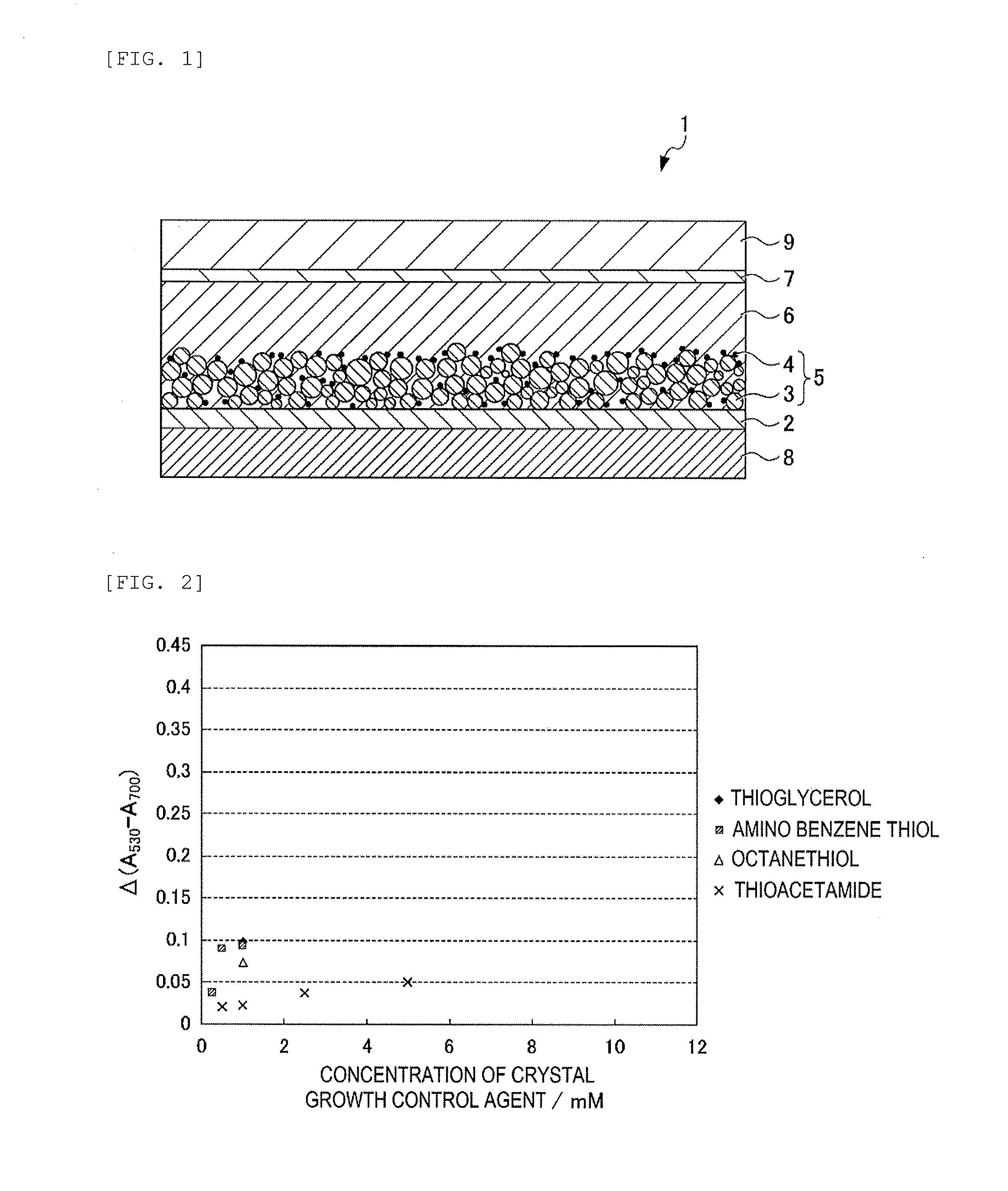
[0121]A copper iodide coating liquid was obtained by dissolving copper iodide in acetonitrile so as to provide a concentration of 0.15 M, and the crystal growth control agent was added and mixed into the obtained solution so as to provide the concentration indicated in Table 1.

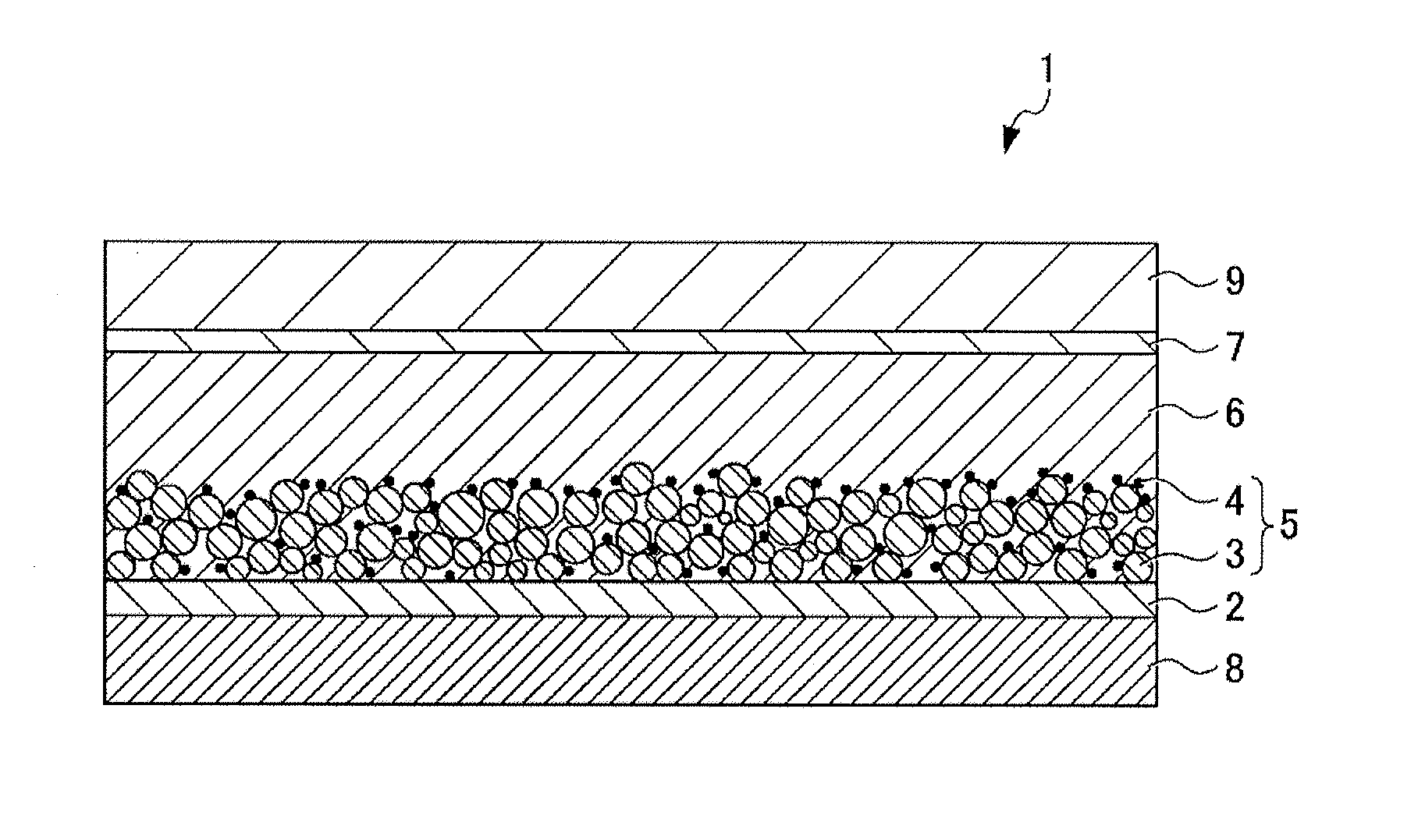
[Create Copper Iodide-Filled Porous Titanium Dioxide Substrate: Filling Porous Titanium Dioxide with Copper Iodide]

[0122]On an FTO layer of a transparent conductive support formed of a glass substrate (thickness: 1,100 μm) and the FTO layer (thickness: 0.8 μm) covering a major one surface of the glass substrate, titanium dioxide paste is screen printed, dried at 150° C., and then heated in an electric furnace at 450° C. Thus, a porous titanium dioxide substrate having a porous titanium dioxide layer provided on the transparent conductive support was prepared.

[0123]The substrate was immersed into an acetonitrile / tert-butyl alcohol solution in wh...

embodiment 2

Regarding Embodiment 2

[Preparation of Copper Iodide Coating Liquid]

[0135]A copper iodide coating liquid was obtained by dissolving copper iodide in acetonitrile such that the concentration was 0.15 M, and the organic salt and the crystal growth control agent were added and mixed into the obtained solution so as to provide the concentration indicated in Table 3.

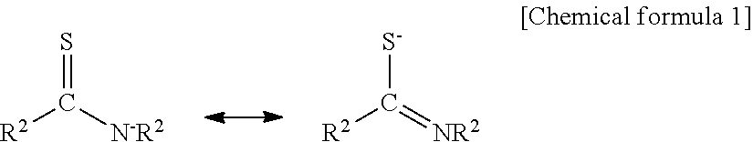
TABLE 3Concentra-tion ofConcentra-Crystalcrystaltion ofgrowthgrowthorganiccontrolcontrolOrganic saltsaltagentagentComparative1-ethyl-3-methyl10 mMNot added0Example 2-1imidazoliumthiocyanateComparative1-ethyl-3-methyl10 mMNot added0Example 2-2imidazoliumbromideExample 2-11-ethyl-3-methyl10 mMDitolyl1 mMimidazoliumdisulfidebromideExample 2-21-ethyl-3-methyl10 mM1,3-1 mMimidazoliumdibutylbromidethioureaComparative1-ethyl-3-methyl10 mMNot added0Example 2-3imidazoliumchlorideExample 2-31-ethyl-3-methyl10 mM1,3-1 mMimidazoliumdibutylchloridethioureaComparative1-ethyl-3-methyl10 mMNot added0Example 2-4imidazoliumdicyanamideExample 2-...


PUM


Abstract

First, there is provided a crystal growth control agent which is capable of suppressing an increase in a crystal size of a p-type semiconductor, and performing chemical modification on a surface of p-type semiconductor microparticle. Second, there is provided a composition for forming a hole transport layer which is capable of prompting crystallization and fine pulverization of the p-type semiconductor and performing the chemical modification on the surface of the p-type semiconductor microparticle even in the case where an organic salt (an ionic liquid) containing an anion other than the thiocyanate ion is used. According to the present invention, the crystal growth control agent contains at least one of sulfur-containing compounds (except for thiocyanate) selected from the group consisting of a compound, which generates a thiolate anion due to dissociation of a proton or a cation, and a disulfide compound, and controls crystal growth of a p-type semiconductor.

Description

TECHNICAL FIELD[0001]The present invention relates to a crystal growth control agent for controlling crystal growth of a p-type semiconductor, a method for forming p-type semiconductor microparticles or a p-type semiconductor microparticle film by using the crystal growth control agent, a composition for forming a hole transport layer of a solar cell, and a solar cell using the composition for forming a hole transport layer.BACKGROUND ARTBackground Art 1[0002]A dye-sensitized solar cell is formed of a working electrode, a porous n-type semiconductor layer including a porous n-type semiconductor (for example, titanium dioxide) on which a dye as a sensitized material is adsorbed, a electrolyte solution containing a redox mediator such as iodine, and a counter electrode. In such a dye-sensitized solar cell, there is a concern of leakage of the electrolyte solution. In this regard, a fully solid dye-sensitized solar cell (hereinafter, also referred to as sDSSC) using a p-type semiconduc...

Claims


Application Information

Patent Timeline
Patent Type & Authority Applications(United States)
IPC IPC(8): H01G9/20
CPCH01G9/2009H01G9/2059H01G9/2022H01G9/2031H01G9/2013Y02E10/542
Inventor NAKAMURA, AKIMASAYAMANOUCHI, ATSUSHIASAI, TAKAHIROISHIKAWA, KAORU
Owner TOKYO OHKA KOGYO CO LTD
Why Eureka
Try Eureka