Process for producing a structure by assembling at least two elements by direct adhesive bonding

a technology of direct adhesive bonding and assembly process, which is applied in the direction of semiconductor devices, semiconductor/solid-state device details, electrical apparatus, etc., can solve the problems of increasing transmission speed, reducing power consumption, and reducing the size of devices

Active Publication Date: 2017-01-26
COMMISSARIAT A LENERGIE ATOMIQUE ET AUX ENERGIES ALTERNATIVES
View PDF16 Cites 4 Cited by
  • Summary
  • Abstract
  • Description
  • Claims
  • Application Information

AI Technical Summary

Problems solved by technology

The three-dimensional integration in microelectronic and nanoelectronic devices reduces the size of the devices, reduces their power consumption, increases the transmission speeds, heightens performance levels and increases the operating frequency, etc.
The drawback of this technique is the implementation of high temperatures (exceeding 250° C.
), which can be incompatible with certain assembled structures.
This

Method used


Image

  • Process for producing a structure by assembling at least two elements by direct adhesive bonding
  • Process for producing a structure by assembling at least two elements by direct adhesive bonding
  • Process for producing a structure by assembling at least two elements by direct adhesive bonding

Examples


Embodiment Construction

[0009]Therefore, one purpose of this invention is to propose a method for producing a structure by assembling at least two elements by direct bonding, wherein the kinetics for enhancing the fracture energy are encouraged at ambient temperature.

[0010]The “enhancing of the fracture energy” is understood as the increase in energy that must be provided to separate the two elements assembled via direct bonding. By encouraging the kinetics for enhancing the fracture energy, the increase in fracture energy is accelerated when compared to the methods of the prior art.

[0011]The aforementioned purpose is achieved by a method for producing a structure by assembling at least two elements by direct bonding, comprising the production of the elements and the assembly of the elements.

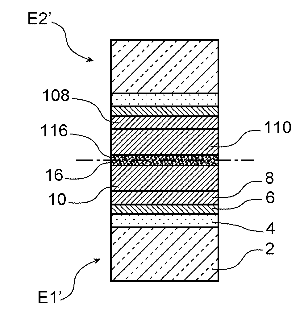
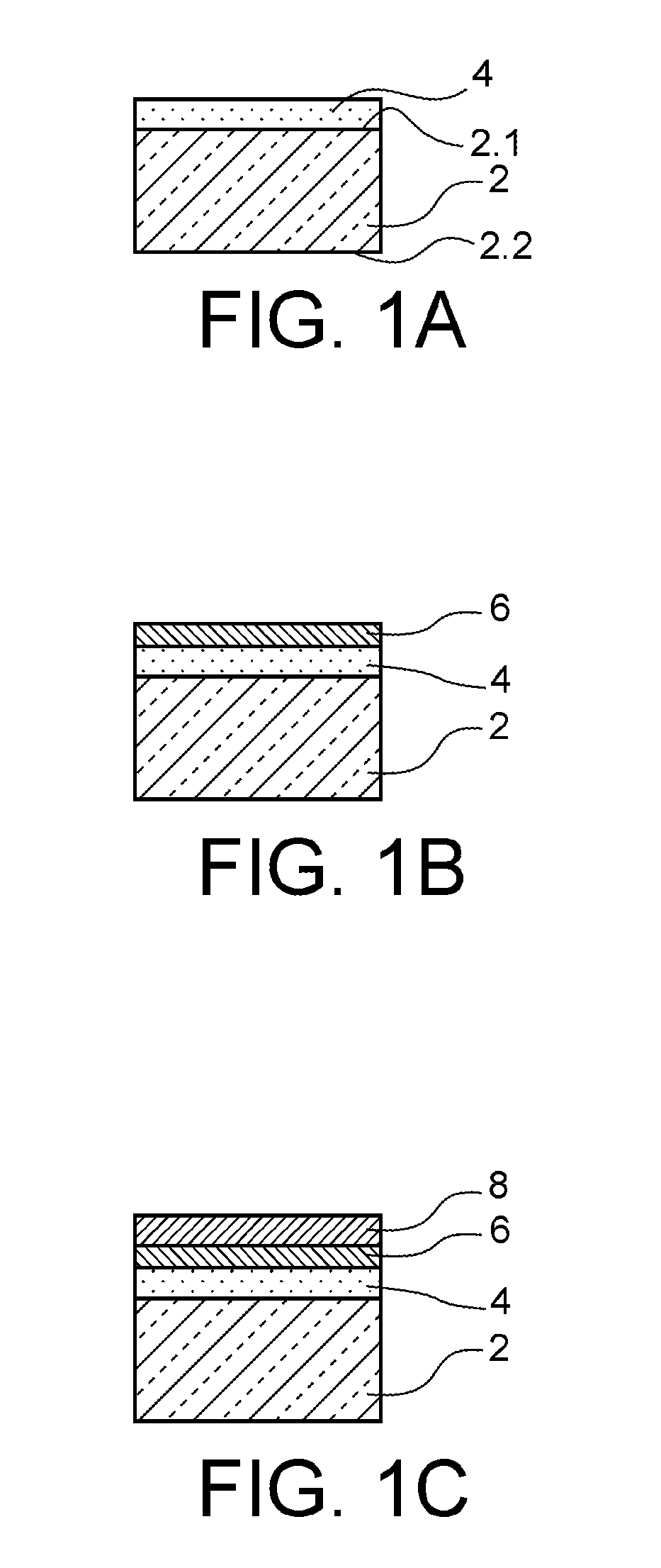
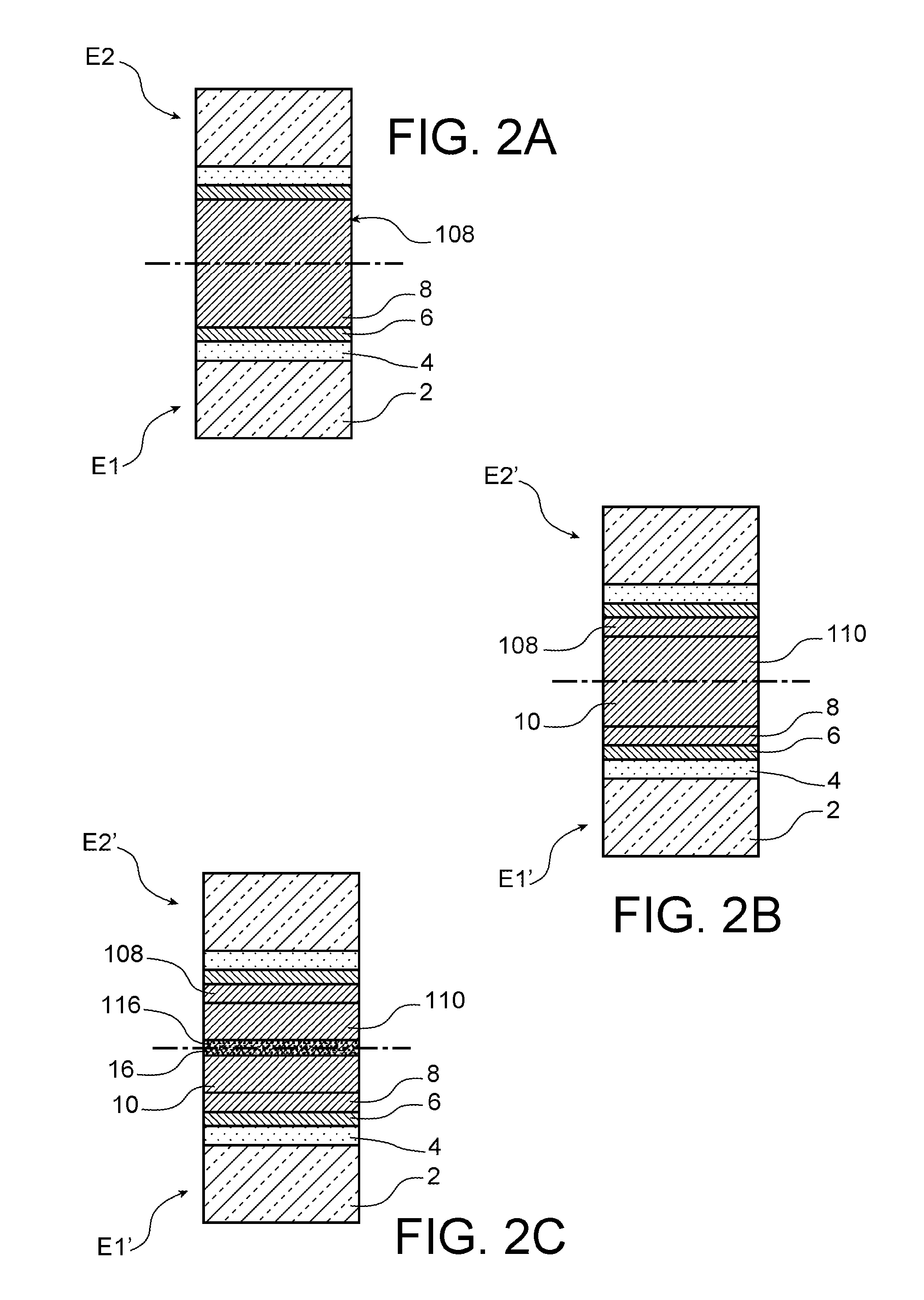
[0012]The production of the elements comprises the following steps:[0013]deposition on a substrate of at least one portion of a given material via physical vapour deposition, forming a growth portion, the given materia...


PUM


Abstract

A method for producing a structure by direct bonding of two elements, the method including: production of the elements to be assembled and assembly of the elements. The production of the elements to be assembled includes: deposition on a substrate of a TiN layer by physical vapor deposition, and deposition of a copper layer on the TiN layer. The assembly of the elements includes: polishing the surfaces of the copper layers intended to come into contact so that they have a roughness of less than 1 nm RMS and hydrophilic properties, bringing the surfaces into contact, and storing the structure at atmospheric pressure and at ambient temperature.

Description

TECHNICAL FIELD AND PRIOR ART[0001]This invention relates to a process for producing a structure by assembling at least two elements by direct bonding, the surface to be assembled of each element comprising at least one copper portion, the method allowing the fracture energy of the structure to be enhanced.[0002]The three-dimensional integration in microelectronic and nanoelectronic devices reduces the size of the devices, reduces their power consumption, increases the transmission speeds, heightens performance levels and increases the operating frequency, etc.[0003]Three-dimensional integration can in particular include the steps of bonding with the alignment of the bonding pads, thinning and vertical interconnection through stacking by means of connection vias. However, in order to obtain a high interconnection density and to simplify the technology, elements are preferably assembled, and in particular connections by metal-metal bonding.[0004]For example, copper is one of the meta...

Claims


Application Information

Patent Timeline
IPC IPC(8): H01L23/00H01L25/065H01L25/00
CPCH01L24/83H01L2224/2755H01L25/0657H01L24/29H01L24/27H01L2225/06524H01L2924/04941H01L2924/04953H01L2224/2745H01L2224/29147H01L2224/27845H01L2224/83895H01L2924/01005H01L2924/01006H01L2924/01015H01L2924/01016H01L2924/01017H01L2924/01008H01L25/50H01L2224/80055H01L2224/80357H01L21/185H01L24/03H01L24/05H01L24/80H01L2224/0345H01L2224/03452H01L2224/0381H01L2224/03845H01L2224/05073H01L2224/0508H01L2224/05147H01L2224/05166H01L2224/05181H01L2224/05184H01L2224/05186H01L2224/05571H01L2224/05647H01L2224/80895H01L2224/80896H01L2224/8083H01L2224/8092H01L2224/80948H01L2224/05547H01L2924/00014H01L2924/049H01L2924/00012H01L24/00
Inventor GONDCHARTON, PAULBENAISSA, LAMINEIMBERT, BRUNOMORICEAU, HUBERT
Owner COMMISSARIAT A LENERGIE ATOMIQUE ET AUX ENERGIES ALTERNATIVES
Why Eureka
Try Eureka