Electroluminescent device

a technology of electron-hole capture and light-emitting diodes, which is applied in the direction of solid-state devices, semiconductor devices, photovoltaic energy generation, etc., can solve the problems of unpractical applications and uneconomical use of large-area displays, and achieve enhanced electron-hole capture, improved radiative recombination, and improved light-emitting

Active Publication Date: 2017-02-23
CAMBRIDGE ENTERPRISE LTD
View PDF7 Cites 24 Cited by
  • Summary
  • Abstract
  • Description
  • Claims
  • Application Information

AI Technical Summary

Benefits of technology

[0017]In order to confine the injected charges (holes and electrons) within the active (emissive) perovskite layer, the PeLED is formed using a thin perovskite film by forming one or both of the charge injecting layers from a material that has a large bandgap relative to the bandgap of the perovskite layer. Without wishing to be bound by theory, it is believed that the small exciton binding energy in the perovskites causes slow electron-hole capture and associated radiative recombination. An important aspect of the invention is the selection of at least one charge injecting layer having a bandgap that is greater than that of the perovskite layer, and with LUMO and HOMO levels correctly selected, so as to achieve spatial confinement of the electrons and holes in the active perovskite layer, resulting in improved radiative recombination and light emission.
[0018]Preferably the perovskite layer is a thin film having a thickness of less than 100 nm; more preferably less than 60 nm, e.g. less than 20 nm. Again without wishing to be bound by theory, it is believed that the confinement of injected charges within the thin “well” enhances electron-hole capture and improves radiative recombination.

Problems solved by technology

However, the fabrication of these devices typically relies on expensive high temperature and high vacuum processes, such as molecular beam epitaxy or thermal sublimation, rendering them uneconomical for use in large area displays.
However, electroluminescence could only be achieved at liquid nitrogen temperatures, rendering those devices impractical for applications.

Method used


Image

  • Electroluminescent device
  • Electroluminescent device
  • Electroluminescent device

Examples


example structure 1

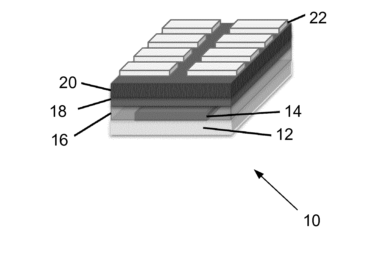
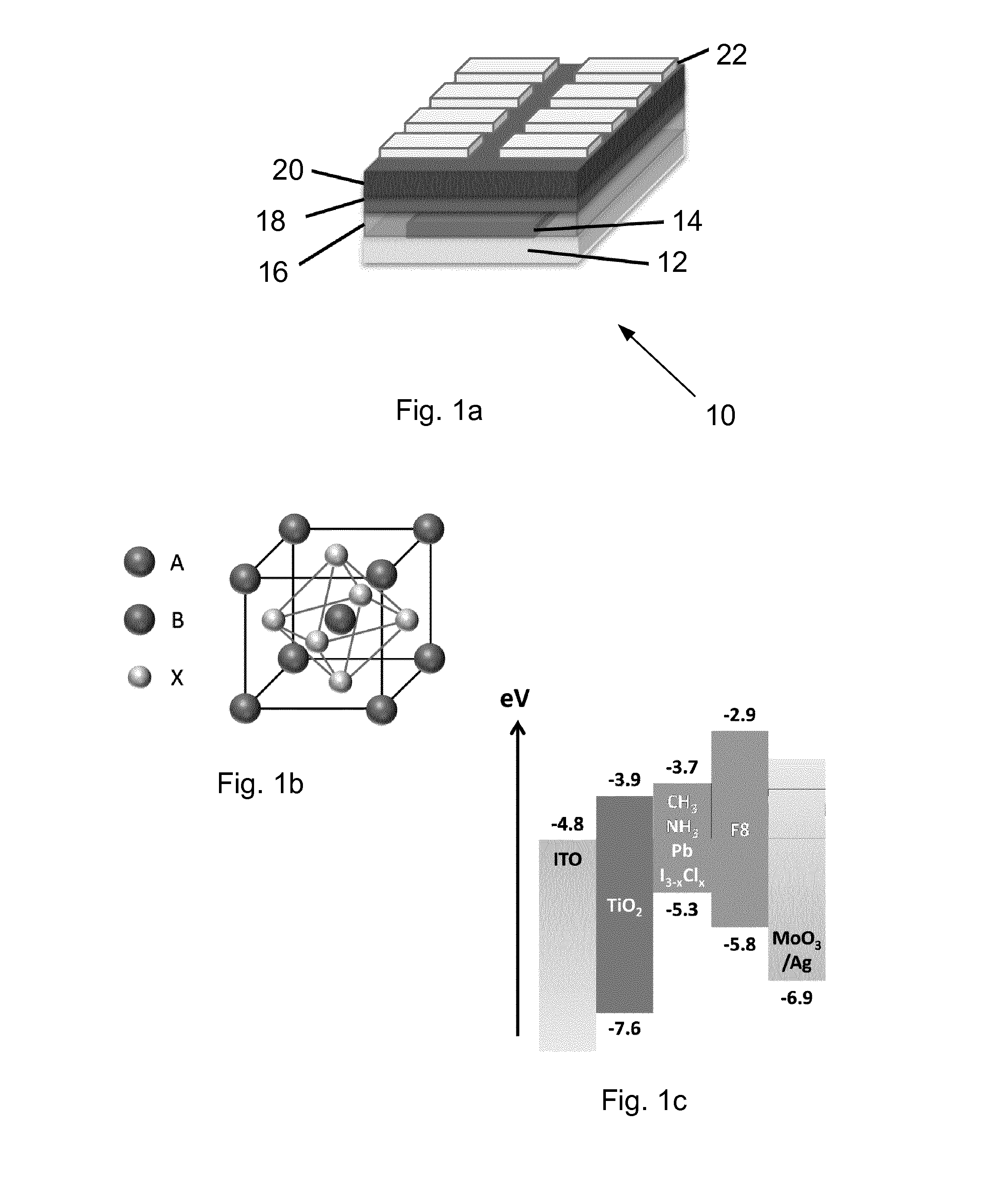
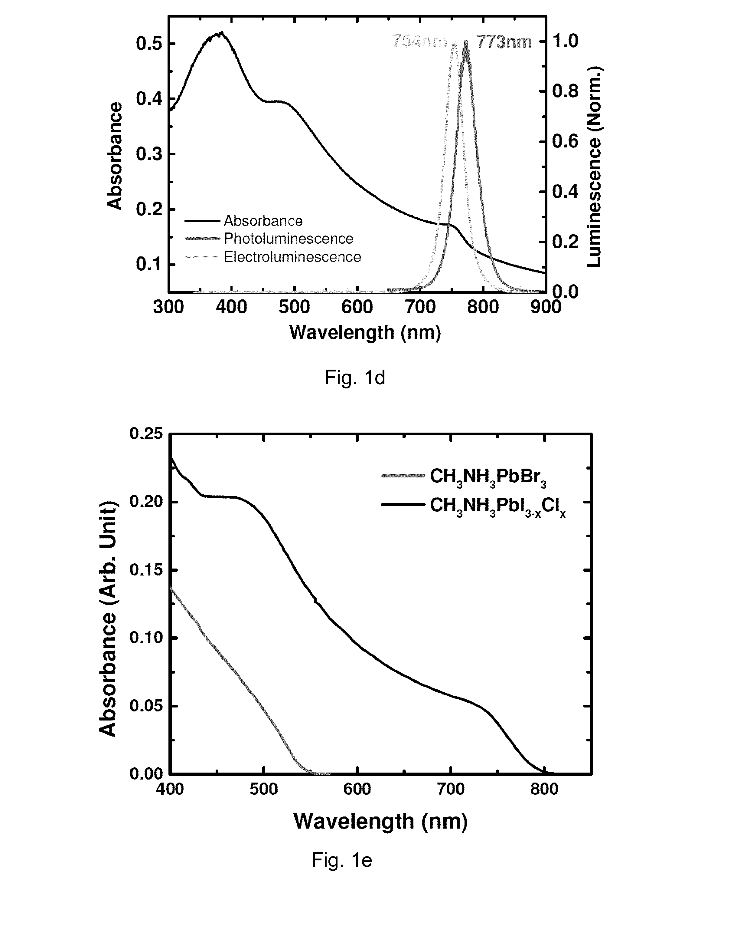
[0095]FIG. 1a shows device architecture 10 according to an embodiment of the invention. The PeLED is fabricated on a transparent substrate 12, which may be a glass substrate. Generally speaking, the PeLED illustrated here comprises a first electrode 14 coupled to a first charge injecting layer 16, a second electrode 22 coupled to a second charge injecting layer 20, and an active layer 18 formed of an organometal halide perovskite material. The active layer 18 is sandwiched between the first and second charge injecting layers 16, 20. One or both of the charge injecting layers 16, 20 may be formed of a semiconductor material, such as titanium dioxide (TiO2). The active perovskite layer may be formed of CH3NH3PbI3-xClx perovskite. Advantageously, the double heterostructure architecture shown here enables the injected charges (holes and electrons) to be confined within the active (emissive) perovskite layer. This may be achieved by forming the PeLED using charge injecting layers 16, 20 ...

example structure 2

[0126]In order to demonstrate the application of organometal halide perovskite as visible light emitters, the larger bandgap CH3NH3PbBr3 perovskite material was used as a green emitter in a PeLED device of the present invention. Since a larger bandgap makes it more difficult to achieve electron injection from TiO2 into the perovskite conduction band, an inverted device structure (relative to that shown in FIG. 1a) was used.

[0127]FIG. 2a shows an example of an inverted device architecture 24. Here, the PeLED is fabricated on a transparent substrate 26, which may be a glass substrate. Generally speaking, the PeLED illustrated here comprises a first electrode 28 coupled to a first charge injecting layer 30, a second electrode 36 coupled to a second charge injecting layer 34, and an active layer 32 formed of an organometal halide perovskite material. The active layer 32 is sandwiched between the first and second charge injecting layers 30, 34. One or both of the charge injecting layers ...

example structure 3

[0136]FIG. 3a shows device architecture 38 according to an embodiment of the invention. The PeLED is fabricated on a transparent substrate 40, which may be a glass substrate. Generally speaking, the PeLED illustrated here comprises a first electrode 42 coupled to a charge injecting layer 44, a second electrode 50, and an active (emissive) layer 48 formed of an organometal halide perovskite material. The active layer 48 is provided between the charge injecting layer 44 and the second electrode 50. In this example device structure, the second electrode 50 directly injects charges into the active perovskite layer 48, and thus can be considered a charge injecting layer. The second electrode 50 may be formed from a conductive material such as Au. The charge injecting layer 44 may be formed from of a semiconductor material, such as titanium dioxide (TiO2) which injects electrons from the first electrode 44 (the anode) into the active perovskite layer. The active perovskite layer may be fo...


PUM

PropertyMeasurementUnit
thicknessaaaaaaaaaa
thicknessaaaaaaaaaa
thicknessaaaaaaaaaa

Abstract

A solid state light-emitting device comprising: a first electrode coupled to a first charge injecting layer; a second electrode coupled to a second charge injecting layer; an emissive layer comprising a perovskite material, wherein the emissive layer is provided between the first and second charge injecting layers; and wherein the bandgaps of the first and second charge injecting layers are larger than the bandgap of the emissive perovskite layer.

Description

FIELD OF THE INVENTION[0001]This invention relates to a solid state light-emitting device, and in particular to a perovskite-based light-emitting diode and related fabrication methods.BACKGROUND TO THE INVENTION[0002]In its most basic form a light emitting diode (LED) comprises a light emitting layer which is positioned between an anode and a cathode. A hole injection layer may be incorporated between the anode and the light emitting layer (also known as the active or emissive layer). It functions to decrease the energy difference between the work function of the anode and the highest occupied molecular orbital (HOMO) of the light emitting layer, thereby increasing the number of holes introduced into the light emitting layer. Broadly speaking, in operation holes are injected through the anode, and if present the hole injection layer, into the active layer, and electrons are injected into the active layer through the cathode. The holes and electrons combine in the light emitting laye...

Claims


Application Information

Patent Timeline
Patent Type & Authority Applications(United States)
IPC IPC(8): H01L51/50H01L51/56H01L51/52
CPCH01L51/5012H01L51/5088H01L51/5092H01L51/5203H01L51/56H01L51/004H01L51/0039H01L51/0037H01L51/0035H01L51/0038H01L51/0072H01L51/0077C08G2261/95C08G2261/512C08G2261/1424C08G2261/3223C08G2261/3221C08G2261/3142H10K85/1135H10K30/151H10K50/11H10K85/60Y02E10/549H10K85/50C08G61/02C08G61/12H10K50/17H10K50/816H10K2101/30H10K2102/351H10K50/171H10K50/805H10K71/00H10K85/30H10K85/111H10K85/114H10K85/115H10K85/141H10K85/6572
Inventor FRIEND, RICHARD HENRYMOGHADDAM, REZA SABERITAN, ZHI KUANGSADHANALA, ADITYALAI, MAY LINGDOCAMPOS, PABLODESCHLER, FELIXPRICE, MICHAELHANUSCH, FABIANSNAITH, HENRY
Owner CAMBRIDGE ENTERPRISE LTD
Why Eureka
Try Eureka