

Fluorescence-based analysis of biopolymers using nanopores
- Summary
- Abstract
- Description
- Claims
- Application Information
AI Technical Summary
Benefits of technology
Problems solved by technology
Method used
Image

Examples
example 1
Materials and Methods
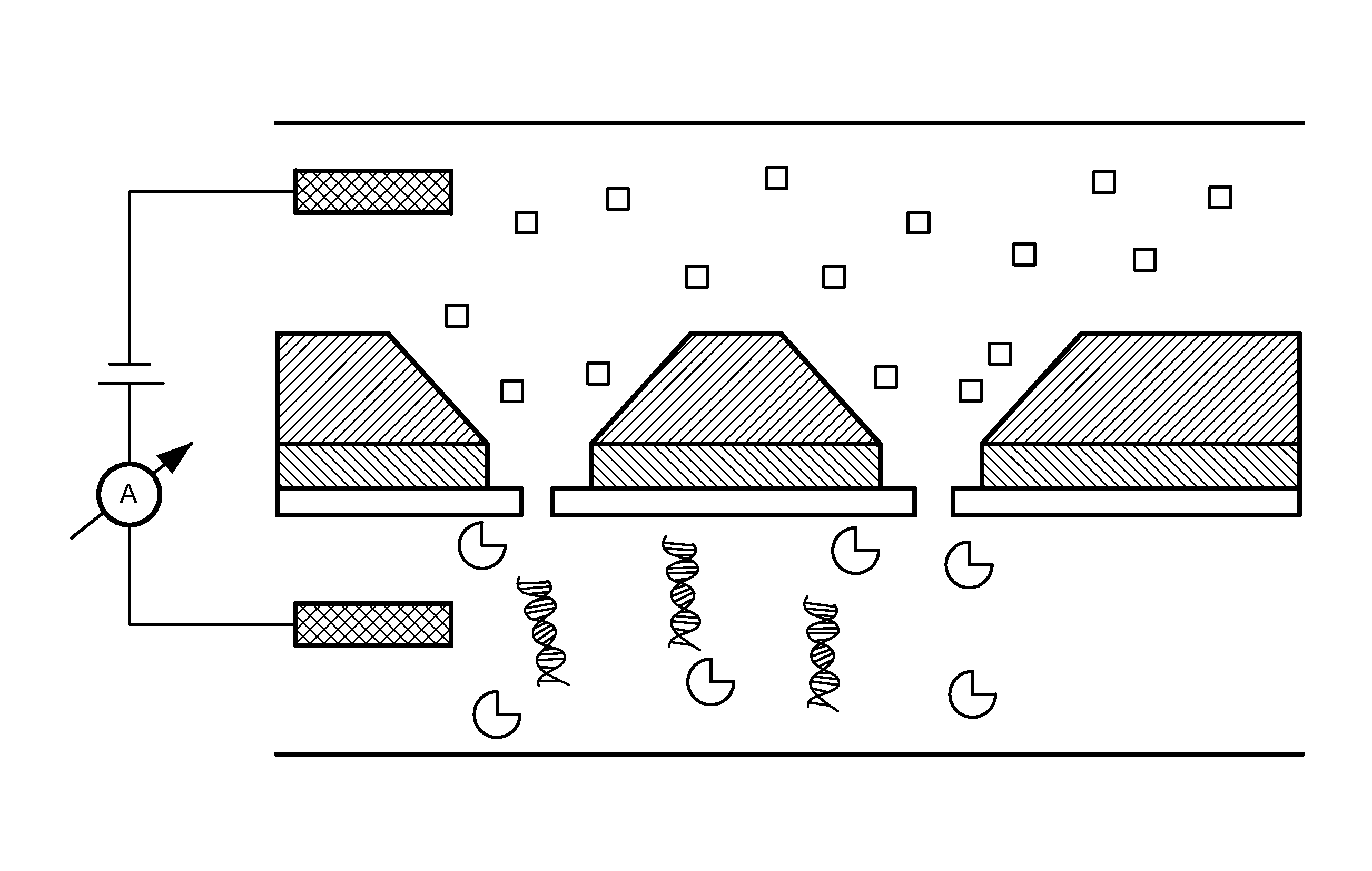
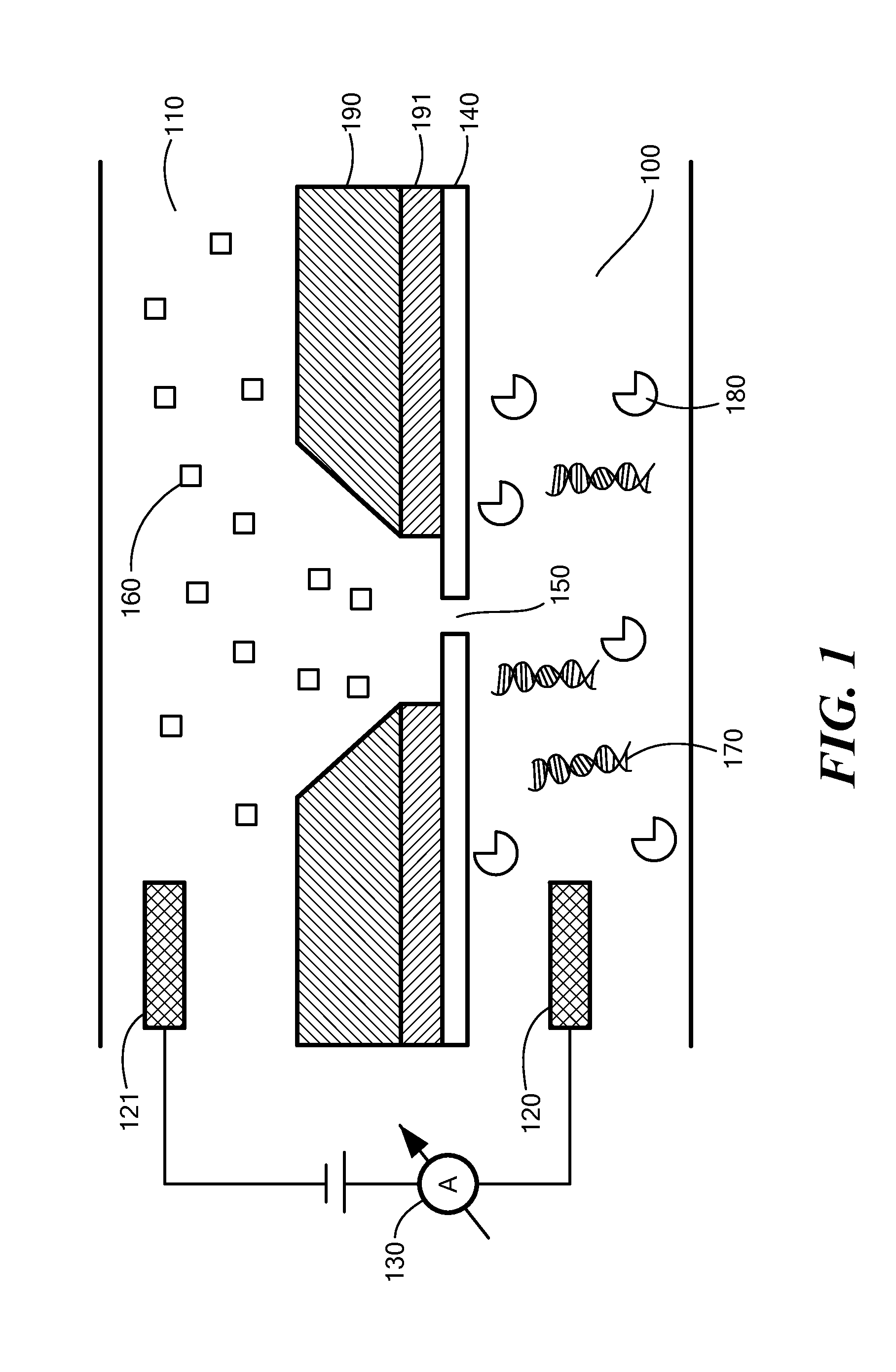
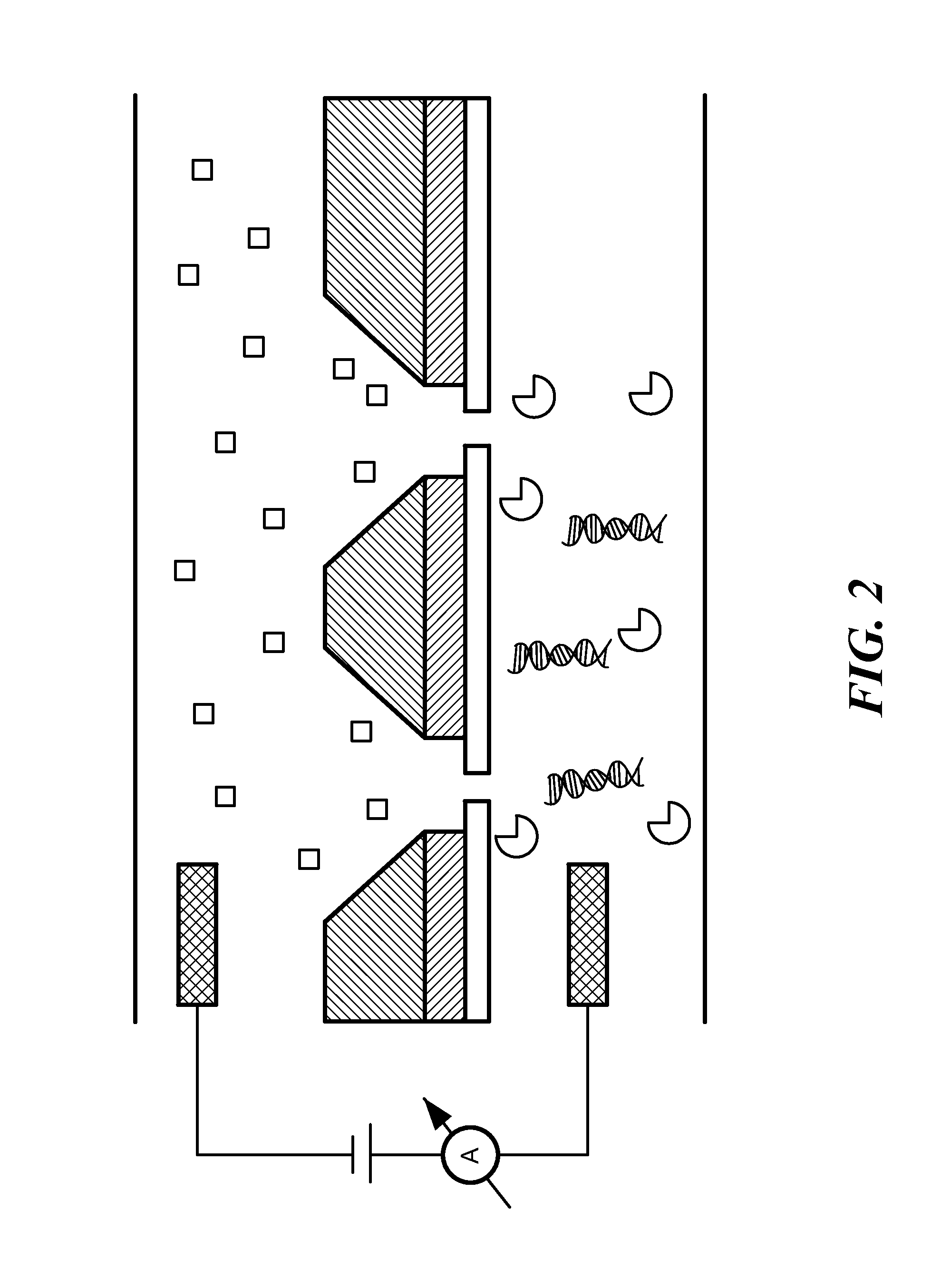
[0062]Nanopores were fabricated in ultrathin silicon nitride membranes as described previously.46 Briefly, a 500-μm-thick silicon wafer with crystal orientation and 2.5 μm of thermal oxide was coated with 100 nm of low-stress chemical vapor deposition silicon nitride (SiN). Standard UV photolithography was used to pattern square openings on one side of the wafer, through which the nitride and oxide were etched using SF6 plasma. The photoresist was stripped, and an anisotropic etch followed by removal of the oxide layer resulted in ˜30 μm×30 μm free-standing windows on the reverse side of the wafer.
[0063]A film of poly(methyl methacrylate) (PMMA) was spun onto the membrane side of the window, and electron-beam lithography was used to pattern an array of small square openings of 800 nm×800 nm or smaller 1.5-3 μm apart. SF6 plasma etch locally thinned the SiN in these regions to 20 nm to increase the signal while maintaining the membrane's mechanical integrity. Th...
example 2
Ca2+ Based Epifluorescence Detection of Unlabeled DNA Molecules Using an Array of Solid-State Nanopores
[0066]A Ca2+ dye solution is flowed underneath the membrane using a flow channel, and ion currents are detected through pores as small as 1.8 nm in diameter at millisecond time-resolutions. The spacing between adjacent pores can be as small as a few micrometers, yielding the pore density on a chip comparable to that of Ion Torrent's device and at least 100×higher than any existing nanopore array device. These experiments are performed at Ca2+ concentrations in which many biological motors, such as the DNA polymerase φ29 remain active. The ionic current information accessed by optical methods is equivalent to that found electrically, and therefore the method paves the way for large-scale parallelization of a wide range of nanopore measurements.
[0067]The system is composed of one or more nanopores formed in a thin insulating silicon nitride membrane, suspended on a silicon chip frame...
PUM
| Property | Measurement | Unit |
|---|---|---|
| Length | aaaaa | aaaaa |
| Length | aaaaa | aaaaa |
| Diameter | aaaaa | aaaaa |
Abstract
Description
Claims
Application Information