Chip-scale two-dimensional optical phased array with simplified controls

a phased array and chip-scale technology, applied in the field of optical phased arrays, can solve the problems of large swap, inconvenient operation, and large power requirements, and achieve the effects of reducing power requirements, compact size, and minimal weigh

Active Publication Date: 2017-09-07
THE UNITED STATES OF AMERICA AS REPRESENTED BY THE SECRETARY OF THE NAVY
View PDF2 Cites 28 Cited by
  • Summary
  • Abstract
  • Description
  • Claims
  • Application Information

AI Technical Summary

Benefits of technology

[0017]An optical phased array (“OPA”) refers to a device having multiple emitters, individual phases of which can be adjusted such that the emitters act in tandem to steer a beam. Applications of chip-scale optical phased arrays according to an embodiment of the invention include beam steering (where light is emitted) and receivers, imagers, or scanners (where light is collected). Chip-scale optical phased arrays according to an embodiment of the invention are advantageous because of their compact size, minimal weight, and reduced power requirements. Such chip-scale optical phased arrays according to an embodiment of the invention are also advantageous because their potentially reduced manufacturing costs enable such devices to find application in areas previously not considered owing to the high cost of prior beam-steering devices. For example, chip-scale optical phased arrays according to an embodiment of the invention are optionally used in automobiles in a manner similar to recently implemented radar systems for collision avoidance. Optical phased arrays according to an embodiment of the invention are optionally used in free-space optical (“FSO”) communication systems.
[0018]Chip-scale devices according to an embodiment of the i

Problems solved by technology

), require significant power (e.g., ˜48 W) and are slow (e.g., <10 Hz); although smaller gimbals with improved performance are available, they are still macro-scale devices.
However, in other applications, the large SWAP is prohibitive and other non-mechanical beam steering solutions are needed.
Limitations of MEMS micromirrors include the limited response time (typically, in the 10 microsecond to millisecond-range) and modest fill-factor (e.g. 30% fill-factor and 7 dB insertion loss) due to the complicated actuator design which requires motion along several axes.
Many optical MEMS components also only function as switches with two stable states (e.g. Texas Instruments' DMD) and are therefore not suitable for beam steering which requires continuously variable devices.
Initial demonstrations have shown the potential of using liquid crystals for up to +/−5° beam steering angles at sub-second response times. More recently, steering angles of +/−40° have been achieved using gratings (with the drawback that these devices are highly polarizati

Method used


Image

  • Chip-scale two-dimensional optical phased array with simplified controls
  • Chip-scale two-dimensional optical phased array with simplified controls
  • Chip-scale two-dimensional optical phased array with simplified controls

Examples


Embodiment Construction

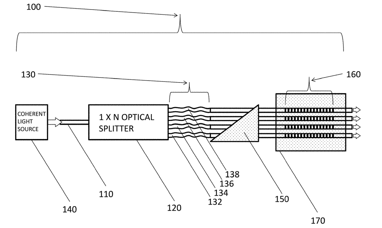
[0034]An embodiment of the invention includes a device 100, as shown by way of example in FIGS. 4 and 5. The device includes an input waveguide 110 operably connected to a 1×N optical splitter 120, which comprises a single splitter input and a plurality of splitter outputs (i.e., N splitter outputs). The plurality of splitter outputs is out of phase and includes a non-uniform phase front. The device 100 includes a one-dimensional phase compensation array 130 communicating with the optical splitter 120. The phase compensation array 130 includes a plurality of N serpentine optical waveguides. (For the purpose of this patent application, the terms serpentine waveguides and S-bend waveguides are equivalent). FIGS. 4 and 5 only shows four serpentine optical waveguides 132, 134, 136, 138 for ease of understanding. However, one of ordinary skill in the art will readily appreciate that the phase compensation array 130 includes as many serpentine optical waveguides as optical splitter 120 ha...


PUM


Abstract

A device includes an optical splitter comprising a plurality of splitter outputs. The splitter outputs are out of phase and include a non-uniform phase front. The device includes a one-dimensional phase compensation array communicating with the optical splitter. The phase compensation array receives the non-uniform phase front and outputs a uniform phase front. The phase compensation array includes a plurality of array outputs. The device includes a tunable linear gradient phase shifter communicating with said phase compensation array to impart a linearly-varying phase shift across said plurality of array outputs, thereby steering a beam along a first angle in a first plane. The device includes a waveguide grating out-coupler communicating with said linear gradient phase shifter, and a uniform phase shifter communicating with the waveguide grating out-coupler. The uniform phase shifter steers the flat phase front along a second angle in a second plane perpendicular to said first plane.

Description

CROSS-REFERENCE TO RELATED APPLICATIONS[0001]The present application claims priority to U.S. Provisional Patent Application Ser. No. 62 / 302,248, which was filed on 2 Mar. 2016.FIELD OF THE INVENTION[0002]The present invention relates in general to optical phased arrays, and in particular to chip-scale optical phased arrays used for optical beam steering (where light is emitted) as well as for optical receivers, imagers and / or scanners (where light is received).BACKGROUND OF THE INVENTIONMechanical Beam Steering Using Gimbals and Fast Steering Mirrors[0003]The simplest method of steering an optical beam is by use of mechanical means. An example of such standard mechanical means includes a standard, macro-scale gimbal 10, such as shown in FIG. 1. A light source and lens mounted on the gimbal 10 enables steering in any direction provided that the gimbal allows for rotation about the two primary axes. Macro-scale gimbals 10 are generally heavy (e.g., ˜20 lbs.), require significant power...

Claims


Application Information

Patent Timeline
IPC IPC(8): G02F1/29G02B6/124G02B6/28
CPCG02F1/292G02F2201/06G02B6/124G02B6/2813G01S7/4813G01S7/4817G02B6/2804G02B6/2821G02F1/2955G02F1/313
Inventor PRUESSNER, MARCEL W.RABINOVICH, WILLIAM S.MAHON, RITAGOETZ, PETER G.
Owner THE UNITED STATES OF AMERICA AS REPRESENTED BY THE SECRETARY OF THE NAVY
Why Eureka
Try Eureka