Sub thz to mid infrared tunable semiconductor plasmonics

a semiconductor plasmonics and semiconductor technology, applied in the field of tunable plasmon resonators, can solve the problems of difficult to achieve the tuning of the plasmon frequency in known metallic structures, and achieve the effect of reducing the cost of manufacturing

Active Publication Date: 2017-09-21
IHP GMBH INNOVATIONS FOR HIGH PERFORMANCE MICROELECTRONICS LEIBNIZ INST FUR INNOVATIVE +1
View PDF0 Cites 5 Cited by
  • Summary
  • Abstract
  • Description
  • Claims
  • Application Information

AI Technical Summary

Benefits of technology

[0016]An advantage of the semiconductor plasmon resonator of the present invention is that it also allows a tuning of the resonator's quality factor. Due to the larger field penetration in semiconductor materials, this is achieved only in semiconductor plasmonics and not in metal plasmonics. This makes the volume of the semiconductor significant which plays the role of tuning the quality factor of the device. In metals, this being a surface phenomenon, volume of the de...

Problems solved by technology

Tuning the plasmon frequency of the plasmons, howe...

Method used


Image

  • Sub thz to mid infrared tunable semiconductor plasmonics
  • Sub thz to mid infrared tunable semiconductor plasmonics
  • Sub thz to mid infrared tunable semiconductor plasmonics

Examples


second embodiment

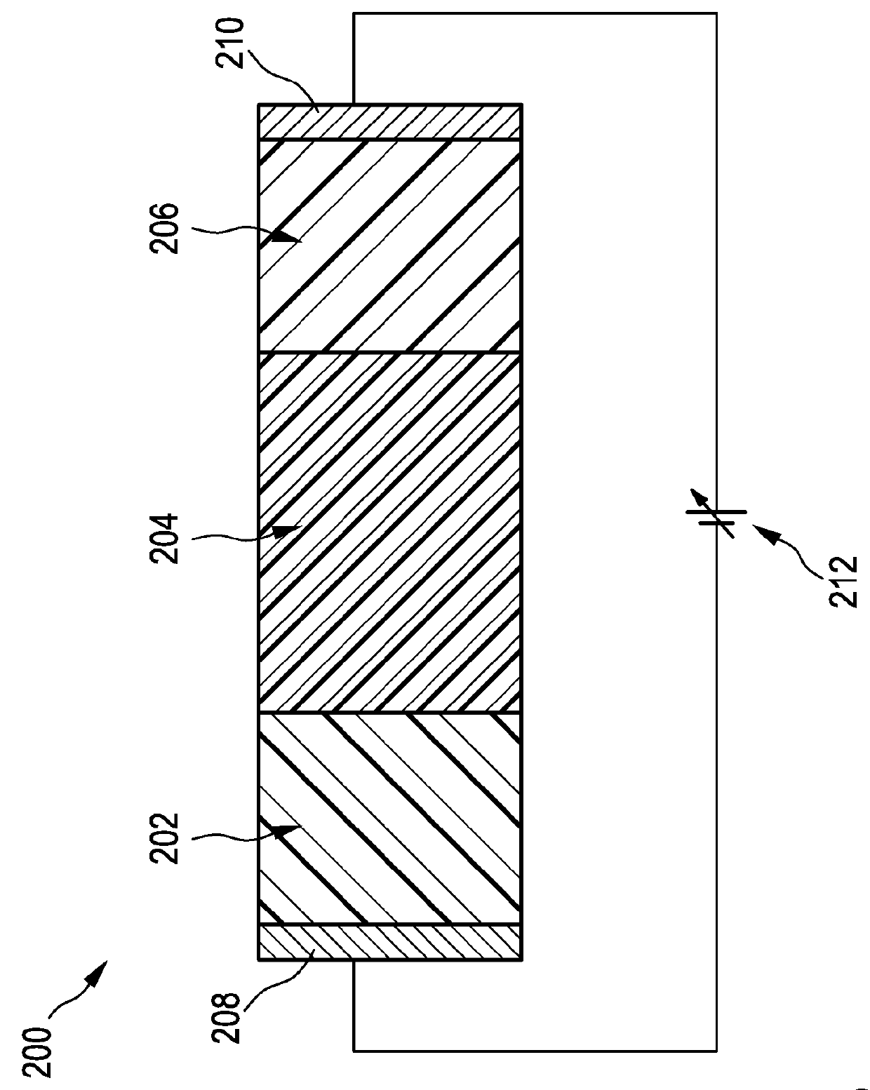
[0072]FIG. 2 is a schematic illustration of a tunable semiconductor plasmon resonator structure 200. The tunable semiconductor plasmon resonator structure 200 of FIG. 2 forms a lateral p-i-n junction with a p-doped semiconductor layer 202, an intrinsic semiconductor layer 204 and an n-doped semiconductor layer 206. In this embodiment, the plasmon resonance layer is formed by the semiconductor layer 204 of intrinsic conductivity, and the integrated tuning device is formed by the p-doped semiconductor layer 202 as a first tuning layer and the n-doped semiconductor layer 206 as a second tuning layer. The tuning layers are connected with respective first and second tuning control electrodes 208 and 210. Thus, the intrinsic semiconductor layer 204 that forms the plasmon resonance layer is laterally embedded between the first and second tuning layers to form a p-i-n structure. This allows controlling concentration of free charge carriers in the intrinsic semiconductor layer 204 in a charg...

third embodiment

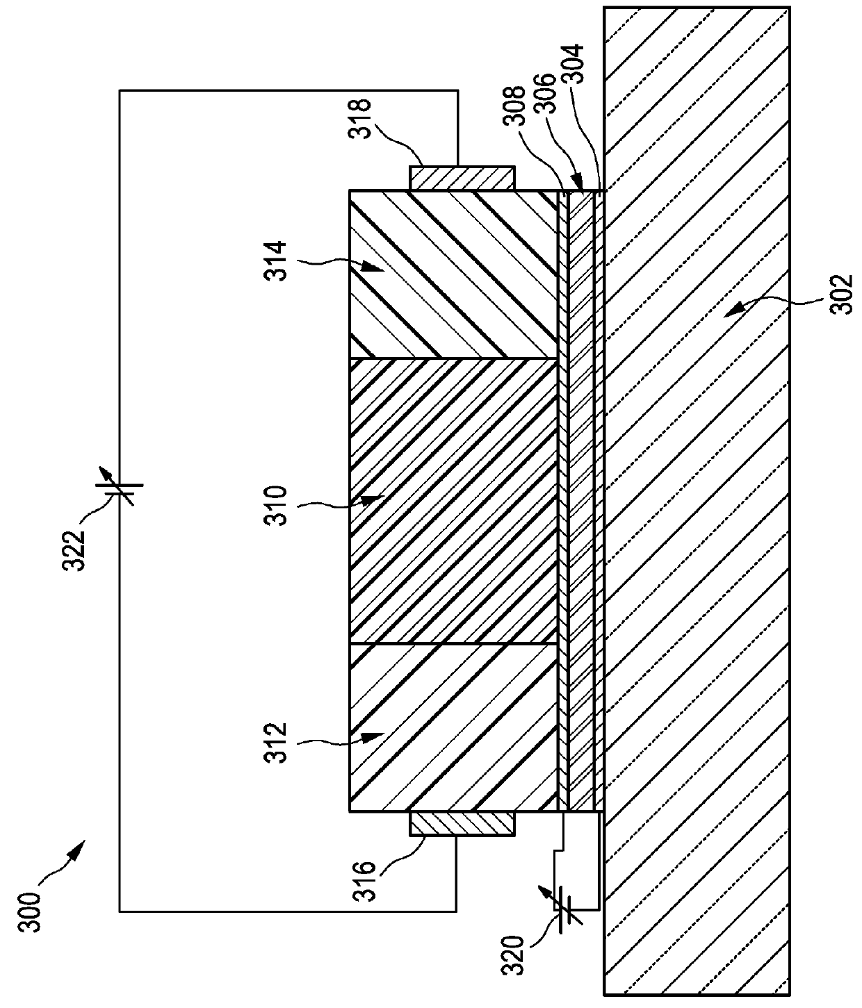
[0076]FIG. 3 is a schematic cross sectional view of a tunable semiconductor plasmon resonator structure 300.

[0077]As with FIGS. 1 and 2, the illustration of the plasmon resonator structure 300 is schematic and simplified in that only the layers that are of importance for explaining the general device structure are shown.

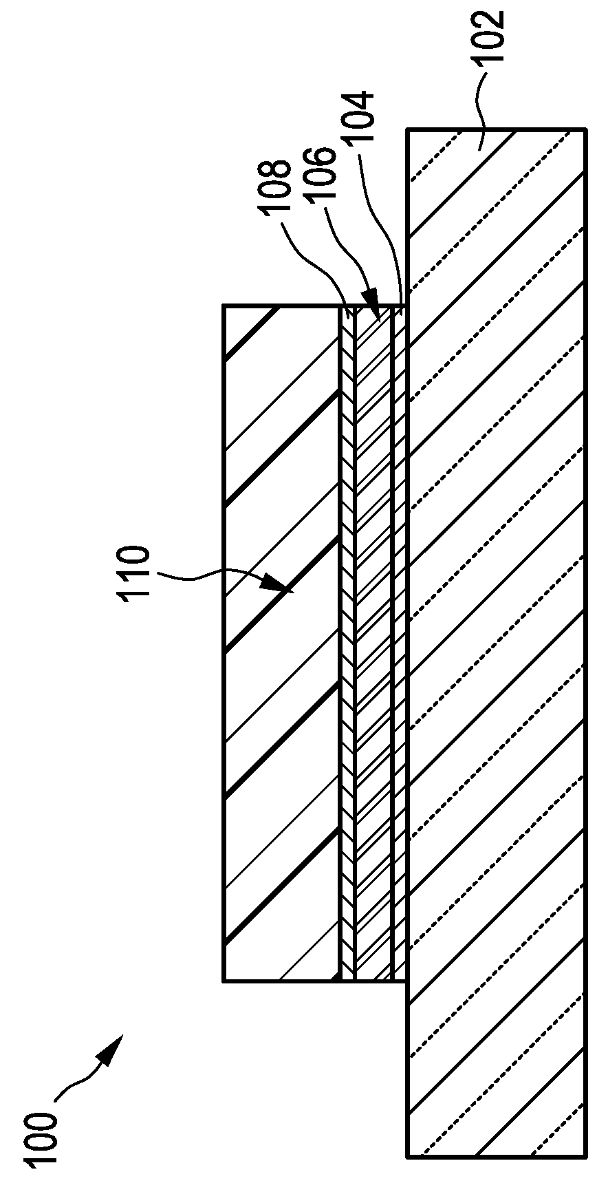
[0078]The plasmon resonator structure 300 is essentially a combination of the embodiments of FIGS. 1 and 2. It comprises a bottom layer 302, a first contact layer 304, a piezoelectric stressor layer 306, and a second contact layer 308. The first and second contact layers 104 and 108 are connectable with an external tuning control device 320, from which they can receive a strain control voltage.

[0079]On the second contact layer 308, a plasmon resonance layer 310 is arranged. The plasmon resonance layer 310 is made of an intrinsic semiconductor material. The plasmon resonance layer 310 is in direct contact with the underlying stack comprising the piezoelectric stressor...

fourth embodiment

[0083]FIG. 4 is a schematic cross sectional view of a tunable semiconductor plasmon resonator structure 400. A plasmon resonance layer 402 is embedded laterally in a lateral p-n junction with a p-doped semiconductor layer 404, and an n-doped semiconductor layer 406. The plasmon resonance layer 402 is made of two different semiconductor layers 402.1 and 402.2 which differ in their material and thus effective mass.

[0084]The present example shows the plasmon resonance layer with two different layers. However, any number of layers can be used to achieve a desired variety of materials in the plasmon resonance layer and thus a desired range of effective masses. Varying the stoichiometry of binary, ternary or quaternary alloys of III-V semiconductors, or of group

[0085]IV semiconductors render orders of magnitude variation in the effective mass, which may additionally be influenced by suitable doping during fabrication.

[0086]The p-doped semiconductor layer 404 forms a first tuning layer and...


PUM


Abstract

A tunable plasmon resonator, comprising a plasmon resonance layer made of graphene, a crystalline group-IV-semiconductor material or a crystalline group-III-V semiconductor material, and arranged on a carrier substrate, the plasmon resonance layer having a plasmon resonance region that is exposed to a sensing volume and a tuning device that is integrated into the plasmon resonator and arranged and configured to modify a density of free charge carriers in the plasmon resonance region or to modify an effective mass amount of the free charge carriers in the plasmon resonance region by applying of a control voltage to tuning control electrode(s) of the tuning device, thereby setting a plasmon frequency of plasmon polaritons in the plasmon resonance region to a desired plasmon frequency value within a plasmon frequency tuning interval, for resonance excitation of plasmon polaritons by incident electromagnetic waves of a frequency corresponding to the set plasmon frequency value.

Description

CROSS REFERENCE TO RELATED APPLICATION[0001]This application claims priority under 35 USC §119 to European Patent Application No. 16 161 267.6 filed on Mar. 18, 2016 and German Patent Application No. 10 2016 206 999.3 filed on Apr. 25, 2016. Both applications are hereby incorporated by reference in their entirety.TECHNICAL FIELD[0002]The present invention relates to a tunable plasmon resonator, a sensor device, to a sensor arrangement, and to a method for fabricating a tunable plasmon resonator.BACKGROUND OF THE INVENTION[0003]In metals, free electrons with an equilibrium electron density exhibit collective longitudinal density oscillations referred to as plasmons having an eigenfrequency called the plasmon frequency. The presence of a boundary formed by a surface gives rise to a further mode of oscillation, namely surface waves forming surface plasmons. Surface plasmons thus are collective oscillations of free electrons at the surface.[0004]Surface plasmons at an interface of a met...

Claims


Application Information

Patent Timeline
IPC IPC(8): G02B5/00G01N21/35G02F1/015G01N21/552
CPCG02B5/008G01N21/553G02F2203/10G02F1/015G01N21/35G01N21/3581
Inventor GUHA, SUBHAJITSCHRODER, THOMASWITZIGMANN, BERNDCAPELLINI, GIOVANNI
Owner IHP GMBH INNOVATIONS FOR HIGH PERFORMANCE MICROELECTRONICS LEIBNIZ INST FUR INNOVATIVE
Why Eureka
Try Eureka