Direct transfer of multiple graphene layers onto multiple target substrates

Inactive Publication Date: 2017-11-23
SABIC GLOBAL TECH BV
View PDF0 Cites 22 Cited by
  • Summary
  • Abstract
  • Description
  • Claims
  • Application Information

AI Technical Summary

Benefits of technology

[0011]A solution to the problems associated with transferring graphene to flexible substrates has been discovered. The solution resides in the ability to increase the graphene transfer process (e.g., by at least 100% or double) by simultaneously utilizing both graphene layers present on a metal catalytic layer in the transfer process while also preserving the graphene layer's properties. Further, the process of the present invention can be performed with or without the use of supporting coatings (e.g., PMMA, PDMS, etc.), solvents, multiple water rinses, or a final thermal annealing step. In particular, two graphene laminates each having a conductive graphene layer and an underlying substrate (e.g., a dielectric or electrical insulator substrate) can be obtained from a single graphene stack (e.g., a CVD produced graphene stack can have a first graphene layer, a second graphene layer, and a catalytic metal layer positioned between the first and second graphene layers) by attaching a first substrate to the fir

Problems solved by technology

However, the complete CVD process is expensive due to the large energy consumption required for the removal of the copper support and transfer of graphene to a dielectric surface or other substrate of interest.
The typical PMMA solvent removal process is incomplete, resulting in detectable residuals with X-Ray Photoelectron Spectroscopy (See, Pirkle et al, Appl. Phys. Lett. 2011, Vol. 99, pp.
The use of PMMA increases the process time and costs as the PMMA is not completely removed.
Residual PMMA, can lead to defective and/or cracked graphene, and therefore, cause problems in creating devices containing graphene from

Method used


Image

  • Direct transfer of multiple graphene layers onto multiple target substrates
  • Direct transfer of multiple graphene layers onto multiple target substrates
  • Direct transfer of multiple graphene layers onto multiple target substrates

Examples


example 1

Process to Produce a Single Graphene Laminate

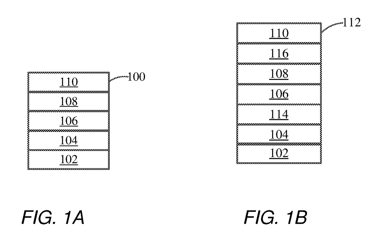
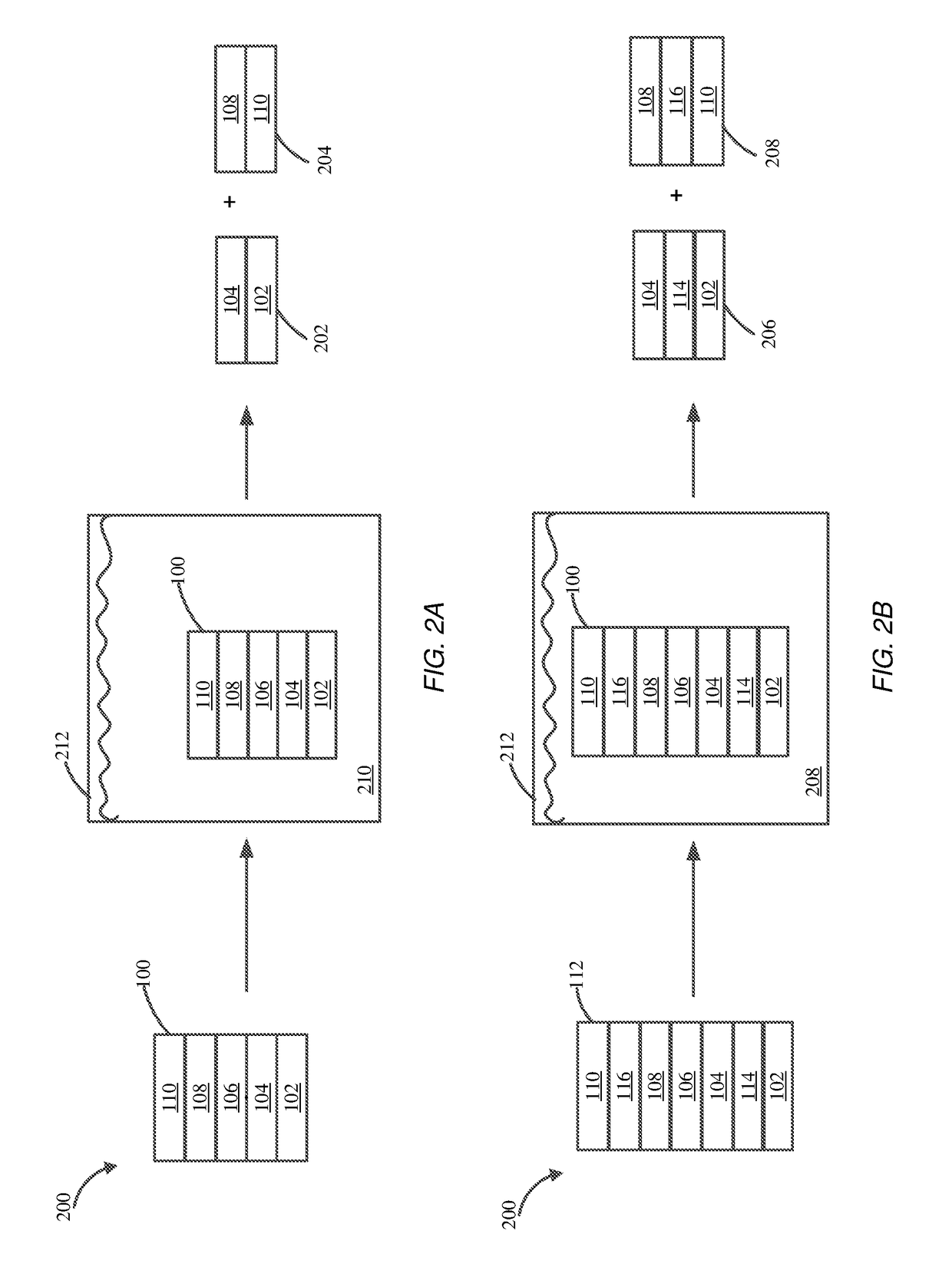
[0067]A layer of paper was inserted in a polyethylene terephthalate (PET) pouch (thickness 75 μm) with the inside surfaces of the pouch coated with heat-activated adhesive. Above the paper, a CVD graphene on copper was placed, and then the pouch was closed. The pouch was passed through a hot commercial laminator. After removal from the laminator the pouch was cooled to room temperature and cut at the borders to obtain two stacks. The first stack included PET, adhesive, graphene and copper. The second stack includes PET, adhesive and paper. The first stack was suspended in an aqueous etching solution of ferric chloride until all the copper was removed. The resulting graphene laminate (PET layer, adhesive layer, graphene layer) was washed with water. The graphene laminate was cut into samples having a dimension of 1×1 cm2 and 2×2 cm2. The sheet resistance of the samples was 1.5-2 kΩ / sq as measured with a 4-probe Van der Paw system (distance...

example 2

Process to Produce Two Graphene Laminates

[0068]A CVD graphene on copper was inserted in a polyethylene terephthalate (PET) pouch (thickness 125 μm) with the inside surfaces of the pouch coated with heat-activated adhesive and then the pouch was closed. The pouch was passed through a hot commercial laminator. After removal from the laminator the pouch was cooled to room temperature and cut at the borders to obtain one stack. The stack included PET, adhesive, graphene, copper, graphene, adhesive, PET. The stack was immersed in an aqueous etching solution of ferric chloride or an aqueous etching solution of hydrochloric acid and hydrogen peroxide until all the copper was removed. The resulting two graphene laminates, each one composed of: a PET layer, adhesive layer, graphene layer, were separated and washed with water. The graphene laminates were cut into samples having a dimension of 1×1 cm2 and 2×2 cm2. The sheet resistance of the samples were 500 Ω / sq-2 kΩ / sq as measured with a 4-p...

example 3

Process to Produce Two Graphene Laminates

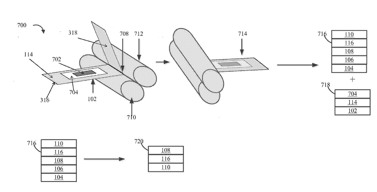
[0069]As shown in FIG. 11, a CVD graphene on copper foil positioned between two pieces of paper was inserted in a polyethylene terephthalate (PET) pouch (thickness 75 μm) with the inside surfaces of the pouch coated with heat-activated adhesive. The pieces of paper covered only a small portion of the sample (about 5 mm), and was not adhered to the surface of the pouch. The pouch was closed, and the pouch was passed through a hot commercial laminator. After removal from the laminator the pouch was cooled to room temperature and the borders were cut and the paper was removed to obtain one stack. The stack included PET, adhesive, graphene, copper, graphene, adhesive, PET. The portion of the CVD graphene that was covered by the paper was not attached to the PET and was used to secure an electrode. The stack was immersed in an aqueous etching solution of ammonium persulfate. A voltage of −5V was applied between the stack and a platinum electrode a...


PUM

PropertyMeasurementUnit
Pressureaaaaaaaaaa
Electrical conductoraaaaaaaaaa

Abstract

Disclosed is a method of making a conductive material or active material that includes graphene or other 2-D materials. The method includes obtaining a layered stack. The layered stack including one or more conductive materials or 2-D materials separated by a metal layer, and one or more substrate materials. The stack can be subjected to a metal removal process to obtain two conductive or active materials. A first conductive or active material can include a first substrate layer attached to the first active layer. The second conductive or active material can include a second substrate layer attached to the second active layer. The first and second active layers can be conductive graphene layers.

Description

CROSS REFERENCE TO RELATED APPLICATIONS[0001]This application claims benefit to U.S. Provisional Patent Application No. 62 / 074,948 titled “DIRECT TRANSFER OF MULTIPLE GRAPHENE LAYERS ONTO MULTIPLE TARGET SUBSTRATES”, filed Nov. 4, 2014. The contents of the referenced application are incorporated into the present application by reference.BACKGROUND OF THE INVENTION[0002]A. Field of the Invention[0003]The invention generally concerns a process for transferring graphene layers and other two dimensional materials from one substrate to another target substrate. The process can be used to simultaneously transfer graphene layers present on both sides of one substrate (e.g., metal substrate or layer) to two separate substrates, thereby increasing the efficiency of the graphene transfer process.[0004]B. Description of Related Art[0005]Graphene is pure carbon in the form of a one atom thick, planar sheet of sp2-bonded carbon atoms that are densely packed in a honeycomb crystal lattice. As a s...

Claims


Application Information

Patent Timeline
IPC IPC(8): H01L29/16B32B7/12B32B9/00B65H20/02B32B37/12B32B3/26H01L21/02C23F1/16H01L21/683B32B15/04
CPCH01L29/1606B65H2301/44318H01L21/02527H01L21/02568B32B7/12C23F1/16B32B3/266B32B15/04B32B37/1207B32B9/007B65H20/02H01L2221/68363B32B2307/202B32B2311/12B32B2311/22H01L21/683H01L21/02422H01L21/6835H01L29/413H01L2221/68359C01B32/194C01B32/182
Inventor TREOSSI, EMANUELESCIDA, ALESSANDRAPALERMO, VINCENZOKHAN, MOHD ADNAN
Owner SABIC GLOBAL TECH BV
Why Eureka
Try Eureka