Advanced Solder Alloys For Electronic Interconnects

a technology of electronic interconnections and alloys, which is applied in the direction of welding/cutting media/materials, manufacturing tools, and soldering apparatus, etc., can solve the problems of generating a lot of heat which needs to be dissipated, the alloy of snag3.0cu0.5 cannot perform well at such temperatures, and the stress fracture of the stressed joint is too early to achieve the effect of improving fatigue life, improving thermal properties, and improving electrical properties

Inactive Publication Date: 2018-04-12
FRY S METALS INC
View PDF1 Cites 16 Cited by
  • Summary
  • Abstract
  • Description
  • Claims
  • Application Information

AI Technical Summary

Benefits of technology

[0016]It is an object of the current invention to provide a solder alloy with improved electrical properties.
[0017]It is an object of the current invention to provide a solder alloy with improved thermal properties.
[0018]It is an object of the current invention to provide a solder alloy with improved fatigue life.
[0019]It is another object of the current invention to provide low contact resistance in an LED die attach layer.
[0020]It is another object of the current invention to provide little to no change in contact resistance of a die attach layer during operation and aging.
[0021]It is an object of the current invention to allow for higher efficiency of an LED or any other high-power electronic device at high power operation.

Problems solved by technology

The thicker intermetallic layers, together with any voids that may have developed, may further contribute to premature fracture of a stressed joint.
The SnAg3.0Cu0.5 alloy does not perform well at such temperatures.
Electronic devices, especially high power devices such as LED and high power amplifiers and switches etc., generate a lot of heat which need to be dissipated.
During operation of such devices, the thermal and electrical interface material sees high temperatures for long periods of time.
During high temperature operation, the interconnect material also faces high mechanical stress due to coefficient of thermal expansion (CTE) miss-match between the device, substrate and interconnect materials.
Changes in conductivity are not desirable.
Resistivity changes in the solder alloys are also undesirable.

Method used


Image

  • Advanced Solder Alloys For Electronic Interconnects
  • Advanced Solder Alloys For Electronic Interconnects
  • Advanced Solder Alloys For Electronic Interconnects

Examples


Embodiment Construction

[0095]The invention relates to micro level additions to solder alloys to engineer the electrical and thermal properties for use in the manufacture of electronic components and devices, as well as in electronic assembly and packaging.

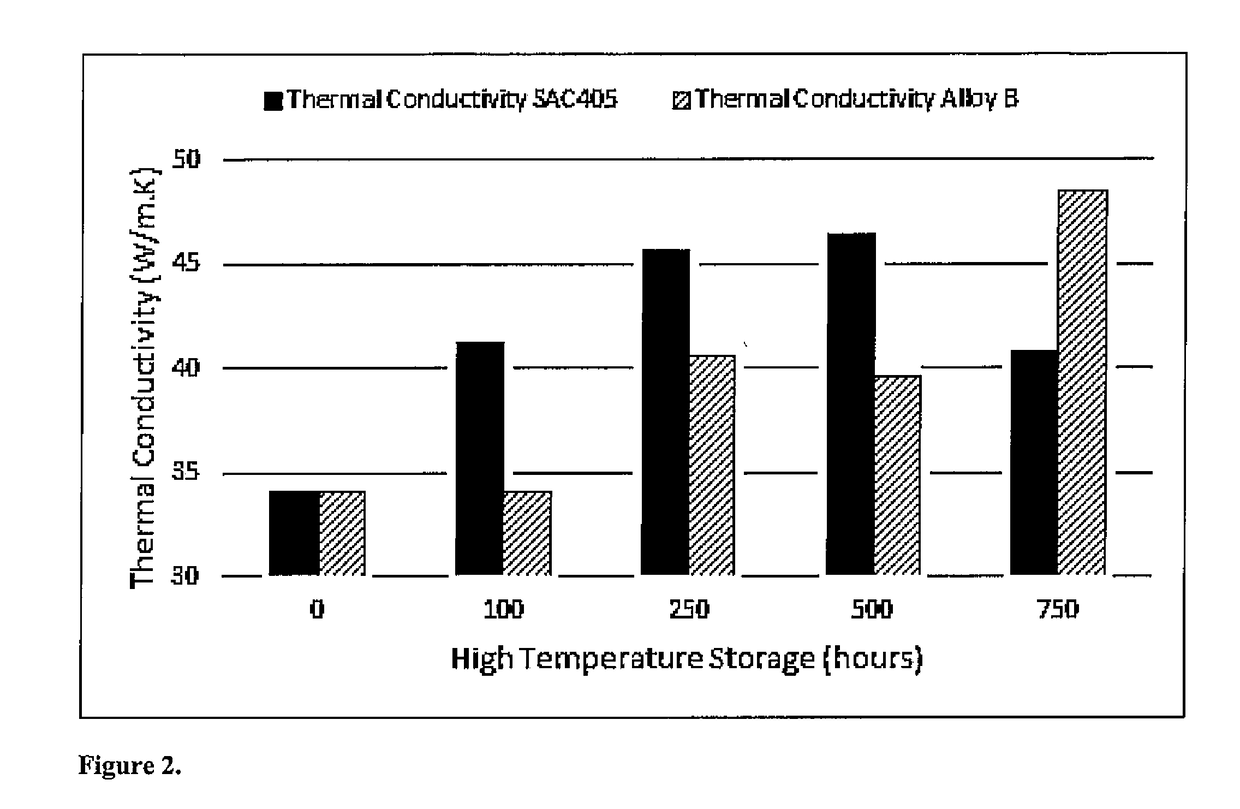
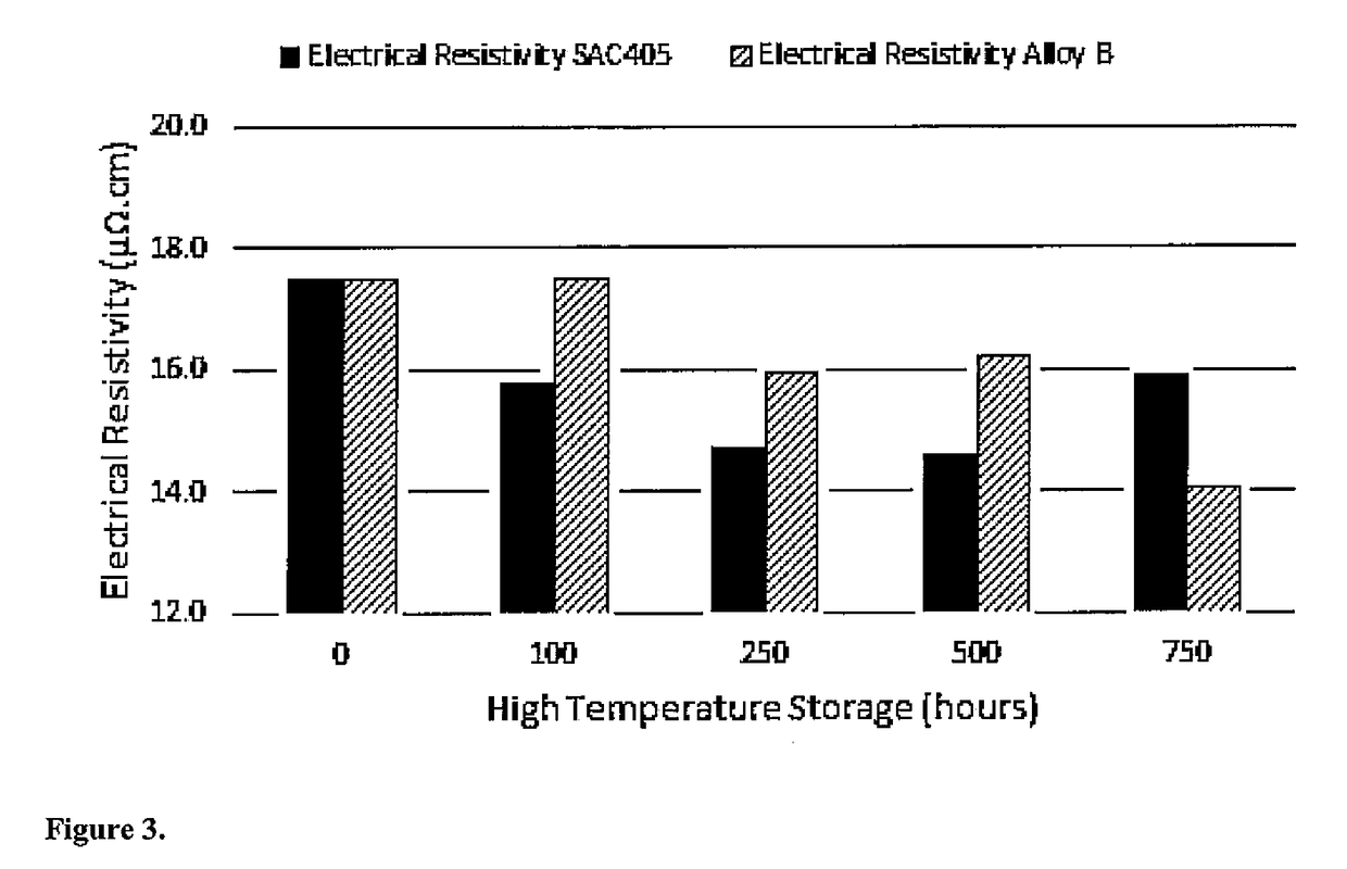
[0096]The novel solder alloys allow for improved electrical properties in addition to improved thermal fatigue life of the die attach layer. The invention results in lower contact resistance in a die attach layer, lower change in contact resistance during operation and aging of the die attach layer, and higher efficiency of LEDs, especially during high power operation.

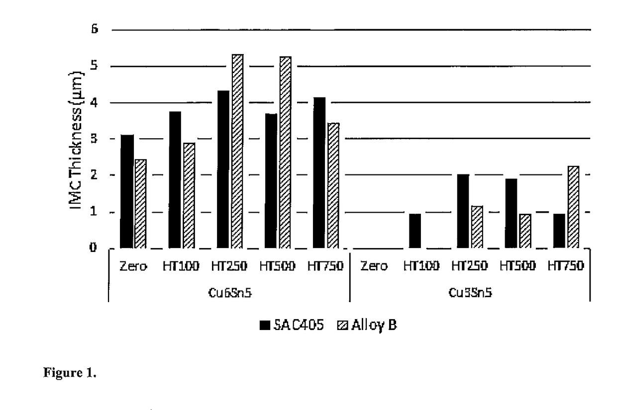
[0097]The engineered microstructure of finer IMC particles in the solder alloy allows for more uniform distribution of the particles compared to SAC alloys. The smaller size of bulk IMCs and their uniform distribution lowers the electronic scattering at interface between IMCs and the adjoining layers.

[0098]The engineered microstructure allows for slower growth of bulk IMCs, controlled inter...


PUM

PropertyMeasurementUnit
melting pointaaaaaaaaaa
temperatureaaaaaaaaaa

Abstract

Improved electrical and thermal properties of solder alloys are achieved by the use of micro-additives in solder alloys to engineer the electrical and thermal properties of the solder alloys and the properties of the reaction layers between the solder and the metal surfaces. The electrical and thermal conductivity of alloys and that of the reaction layers between the solder and the -metal surfaces can be controlled over a wide range of temperatures. The solder alloys produce stable microstructures wherein such stable microstructures of these alloys do not exhibit significant changes when exposed to changes in temperature, compared to traditional interconnect materials.

Description

FIELD OF THE INVENTION[0001]The invention generally relates to a method for improving the electrical and thermal properties of solder alloys used for LED / Power Semiconductors die attach and component attach.BACKGROUND OF THE INVENTION[0002]There are a wide variety of known soldering techniques in the electronics industry. Wave soldering is a widely used method of mass soldering electronic assemblies. It may be used, for example, for through-hole circuit boards, where the board is passed over a wave of molten solder, which laps against the bottom of the board to wet the metal surfaces to be joined.[0003]Another soldering technique involves printing of the solder paste on the soldering pads on the printed circuit boards followed by placement and sending the whole assembly through a reflow oven. During the reflow process, the solder melts and wets the soldering surfaces on the boards as well as the components.[0004]Another soldering process involves immersing printed wiring boards into...

Claims


Application Information

Patent Timeline
Patent Type & Authority Applications(United States)
IPC IPC(8): H01L33/62H01L23/00H01L33/64B23K1/00B23K1/08B23K1/002B23K1/005B23K35/26C22C13/02
CPCH01L33/62H01L2924/12041H01L24/29H01L33/641H01L33/647B23K1/0016B23K1/085B23K1/002B23K1/0056B23K35/262C22C13/02H01L2933/0066H01L2224/13211H01L2224/13313H01L2224/13339H01L2224/13347H01L2224/1332H01L2224/13355H01L2924/01058H01L2224/29211H01L2224/29313H01L2224/2932H01L2224/29339H01L2224/29347H01L2224/29355H01L2924/20106H01L2924/014H01L24/13H01L2924/351H01L2224/32507H01L2224/32503H01L24/32H01L2224/29111H01L2224/29311H01L2224/29294H01L24/16H01L2224/16503H01L2224/16507H01L2224/13111H01L2224/05647H01L2224/29199H01L2224/83447H01L2924/01047H01L2924/01083H01L2924/01051H01L2924/01029H01L2924/01022H01L2924/01025H01L2924/01024H01L2924/01032H01L2924/01026H01L2924/01013H01L2924/01015H01L2924/01079H01L2924/01031H01L2924/01052H01L2924/01034H01L2924/0102H01L2924/01023H01L2924/01042H01L2924/01078H01L2924/01012H01L2924/01105H01L2924/0103H01L2924/01027H01L2924/01028H01L2924/01049H01L2924/01066H01L2924/00014
Inventor DE AVILA RIBAS, MORGANACHOUDHURY, PRITHASARKAR, SIULIPANDHER, RANJITHERRICK, NICHOLAS G.PATEL, AMITBHATKAL, RAVINDRA MSINGH, BAWA
Owner FRY S METALS INC
Why Eureka
Try Eureka