Dopant introduction method and heat treatment method

a technology of introduction method and heat treatment method, which is applied in the direction of furnace type, semiconductor device, furnace, etc., can solve the problems of difficult heat treatment process, damage to the inside of the semiconductor substrate, and difficulty in a conventionally dominant ion implantation method to implant, and achieve the effect of high activation ra

Active Publication Date: 2018-06-14
DAINIPPON SCREEN MTG CO LTD
View PDF3 Cites 7 Cited by
  • Summary
  • Abstract
  • Description
  • Claims
  • Application Information

AI Technical Summary

Benefits of technology

[0015]It is therefore an object of the present invention to introduce a necessary and sufficient dopant without producing any defect and to provide a high activation rate.

Problems solved by technology

In such a three-dimensional structure, it is difficult for a conventionally dominant ion implantation method to implant a dopant into a required location in some cases.
The ion implantation also has the problem of damaging the inside of the semiconductor substrate during the implantation to produce crystal defects.
Unfortunately, a native oxide film is inevitably formed on the surface of the semiconductor substrate at the time of the deposition of the PSG film or the like.
It is difficult for such heat treatment processes for an extremely short time period such as flash lamp annealing to diffuse the sufficient dopant from the film containing the dopant through the oxide film into the semiconductor substrate.
Spike RTA (Rapid Thermal Annealing) that is a longer-time heat treatment process than the flash lamp annealing can be used to diffuse the dopant through the oxide film into the semiconductor substrate, but presents the problem of the low activation rate of the diffused dopant.
In addition, there is a danger that the spike RTA causes the dopant to diffuse from the surface of the semiconductor substrate to an excessive depth.

Method used


Image

  • Dopant introduction method and heat treatment method
  • Dopant introduction method and heat treatment method
  • Dopant introduction method and heat treatment method

Examples


first preferred embodiment

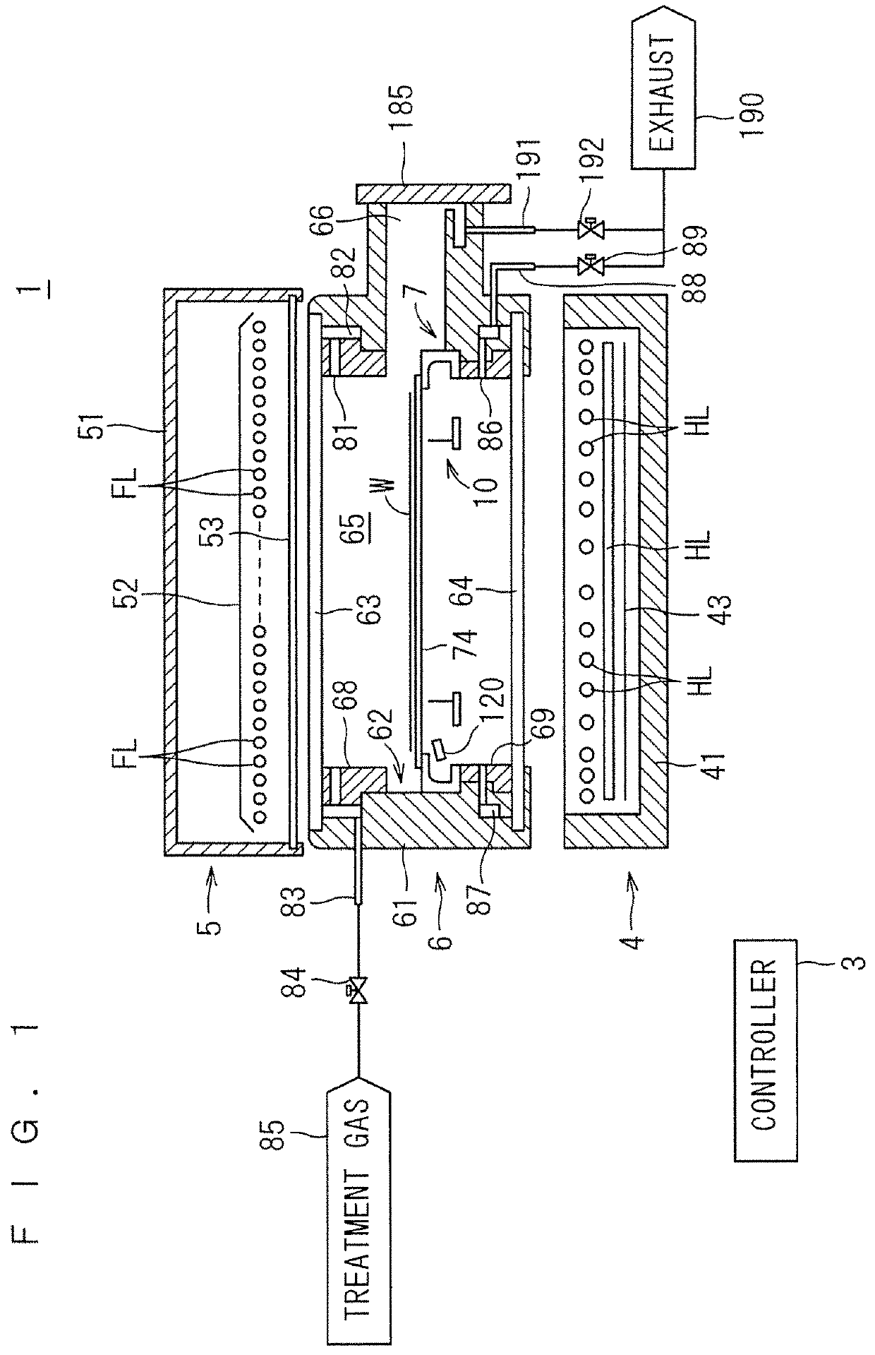
[0032]First, a heat treatment apparatus which performs a heat treatment required when performing a dopant introduction method according to the present invention will be described. FIG. 1 is a longitudinal sectional view showing a configuration of a heat treatment apparatus 1 used for the dopant introduction method and a heat treatment method according to the present invention. The heat treatment apparatus 1 of FIG. 1 is a flash lamp annealer for irradiating a disk-shaped semiconductor wafer W serving as a substrate with flashes of light to heat the semiconductor wafer W. The size of the semiconductor wafer W to be treated is not particularly limited. For example, the semiconductor wafer W to be treated has a diameter of 300 mm and 450 mm. It should be noted that the dimensions of components and the number of components are shown in exaggeration or in simplified form, as appropriate, in FIG. 1 and the subsequent figures for the sake of easier understanding.

[0033]The heat treatment ap...

second preferred embodiment

[0098]Next, a second preferred embodiment according to the present invention will be described. The heat treatment apparatus 1 according to the second preferred embodiment is identical in overall configuration with that according to the first preferred embodiment. The procedure for the treatment of a semiconductor wafer W in the heat treatment apparatus 1 according to the second preferred embodiment is also substantially similar to that according to the first preferred embodiment. The second preferred embodiment differs from the first preferred embodiment in that the heat treatment process is performed in a reduced-pressure condition.

[0099]Although the heat treatment process of the semiconductor wafer W is performed in an ordinary-pressure nitrogen atmosphere in the first preferred embodiment, the rapid heating and flash heating of the semiconductor wafer W are performed in a reduced-pressure condition of not greater than 100 Torr (approximately 13330 Pa) in the second preferred emb...

third preferred embodiment

[0101]Next, a third preferred embodiment according to the present invention will be described. The heat treatment apparatus 1 according to the third preferred embodiment is identical in overall configuration with that according to the first preferred embodiment. The procedure for the treatment of a semiconductor wafer W in the heat treatment apparatus 1 according to the third preferred embodiment is also substantially similar to that according to the first preferred embodiment. The thin film 21 of PSG is deposited on the front surface of the semiconductor wafer W. The third preferred embodiment differs from the first preferred embodiment in atmosphere in the chamber 6 during the execution of the heat treatment process.

[0102]Although the heat treatment process of the semiconductor wafer W is performed in an ordinary-pressure nitrogen atmosphere in the first preferred embodiment, the rapid heating using the halogen lamps HL is performed in a hydrogen-containing atmosphere and the flas...


PUM

PropertyMeasurementUnit
pressureaaaaaaaaaa
diameteraaaaaaaaaa
diameteraaaaaaaaaa

Abstract

A thin film containing a dopant is deposited on a surface of a semiconductor wafer. The semiconductor wafer on which the thin film containing the dopant is deposited is rapidly heated to a first peak temperature by irradiation with light from halogen lamps, so that the dopant is diffused from the thin film into the surface of the semiconductor wafer. The thermal diffusion using the rapid heating achieves the introduction of the necessary and sufficient dopant into the semiconductor wafer without producing defects. The surface of the semiconductor wafer is heated to a second peak temperature by further irradiating the semiconductor wafer with flashes of light from flash lamps, so that the dopant is activated. The flash irradiation which is extremely short in irradiation time achieves a high activation rate without excessive diffusion of the dopant.

Description

BACKGROUND OF THE INVENTIONField of the Invention[0001]The present invention relates to a dopant introduction method and a heat treatment method which introduce a dopant into a semiconductor substrate to activate the dopant.Description of the Background Art[0002]In the process of manufacturing a semiconductor device, the introduction of a dopant into monocrystalline silicon or germanium is an essential step. An n-type semiconductor or a p-type semiconductor is produced by the introduction of a dopant. The introduction of a dopant is typically achieved by ion-implanting dopant atoms such as boron (B), arsenic (As) and phosphorus (P) into a semiconductor substrate of silicon and the like and then performing an annealing process on the semiconductor substrate to activate the dopant atoms.[0003]In recent years, an attempt has been made to improve device performance by changing a conventional planar device structure to a three-dimensional structure (for example, a FinFET). In such a thre...

Claims


Application Information

Patent Timeline
Patent Type & Authority Applications(United States)
IPC IPC(8): H01L21/225H01L21/324H01L21/02
CPCH01L21/2256H01L21/324H01L21/02129H01L21/67115H01L29/78H01L29/66575F27B17/0025H01L21/2255H01L21/2686H01L21/68707H01L21/6875H01L21/0257
Inventor FUSE, KAZUHIKOTANIMURA, HIDEAKIKATO, SHINICHI
Owner DAINIPPON SCREEN MTG CO LTD
Why Eureka
Try Eureka