Pi-orbital semiconductor quantum cell

a quantum cell and orbital semiconductor technology, applied in semiconductor devices, solid-state devices, nuclear engineering, etc., can solve the problems of low conversion efficiency of nuclear energy to electric energy between two types of nuclear batteries, and achieve the effects of reducing the carrier concentration, increasing the collection efficiency of electron-hole pairs, and increasing the width of a depletion region

Active Publication Date: 2018-07-26
CHEN BOR RUEY
View PDF0 Cites 8 Cited by
  • Summary
  • Abstract
  • Description
  • Claims
  • Application Information

AI Technical Summary

Benefits of technology

[0017]An objective of the present invention is to provide a quantum cell to enhance nuclear energy to electric energy conversion efficiency of a prior nuclear battery.
[0019]According to the present invention, the N-type π-orbital semiconductor substrate and the N-type π-orbital semiconductor epitaxy layer can lower the carrier concentration in the epitaxy layer, increase the width of a depletion region, and increase the collection efficiency for an electron-hole pair. As such, the open-circuit voltage and the conversion efficiency of the cell are enhanced. The quantum cell further has the following features:

Problems solved by technology

With the fact that current research on the nuclear battery is not enough, nuclear energy to electric conversion efficiency of the two types of nuclear battery is low (0.1-5% for thermal converter; 6-8% for non-thermal converter).

Method used


Image

  • Pi-orbital semiconductor quantum cell
  • Pi-orbital semiconductor quantum cell
  • Pi-orbital semiconductor quantum cell

Examples


Embodiment Construction

[0028]The detailed description and preferred embodiments of the invention will be set forth in the following content, and provided for people skilled in the art so as to understand the characteristics of the invention.

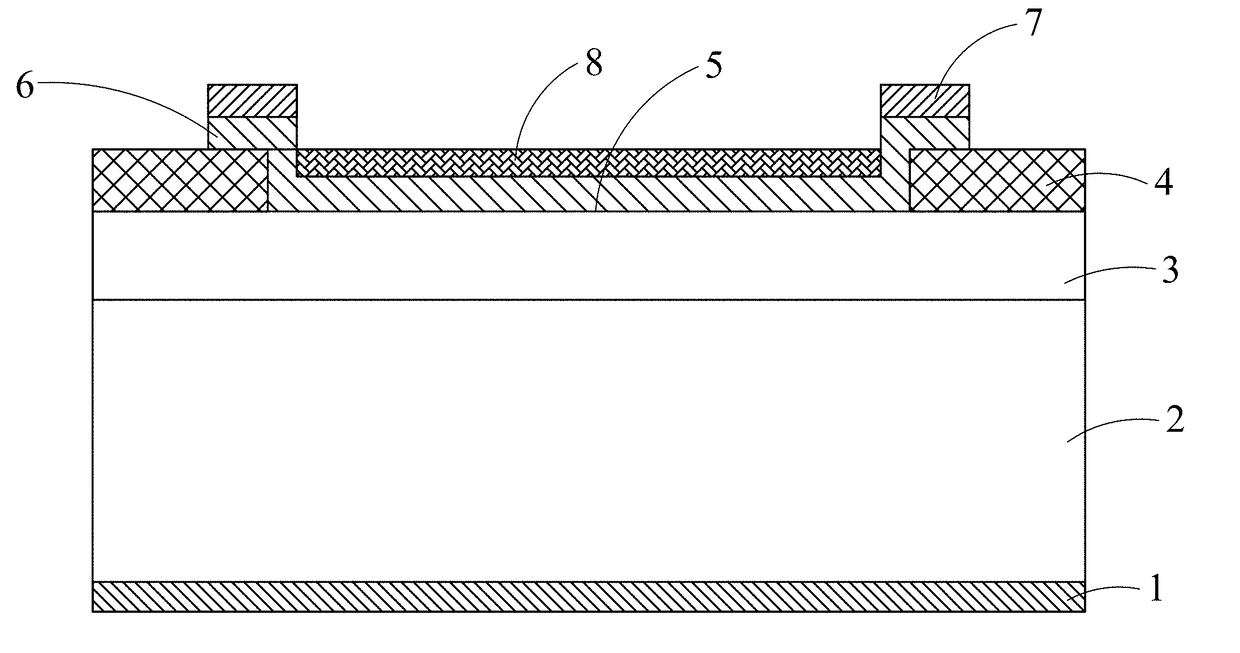
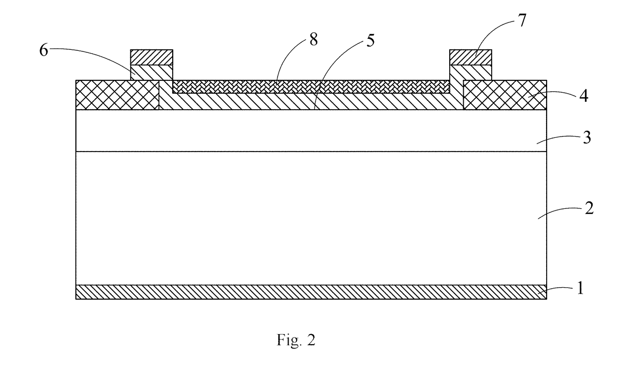
[0029]Referring to FIGS. 2 and 3, a quantum cell is disclosed in an embodiment of the present invention, and the cell comprises: an N-type ohmic contact electrode (1), an N-type π-orbital semiconductor substrate (2), an N-type π-orbital semiconductor epitaxy layer (3), a SiO2 passivation layer (4), a graphite contact layer (5), a Schottky contact electrode (6), a binding layer (7), and a radioisotope layer (8). The N-type π-orbital semiconductor substrate (2) includes an organic semiconductor material with an aromatic group or a semiconductor material with a carbon-carbon bond. The N-type π-orbital semiconductor epitaxy layer (3) has a doping concentration of 1×10¹³-5×1014 cm−3 and is formed by injection of a cationic complex in a dose of 6×10¹³-1×1015 cm−3.

[0030]The N...


PUM


Abstract

Herein is disclosed a quantum cell from top to down including: an N-type ohmic contact electrode, an N-type π-orbital semiconductor substrate, an N-type π-orbital semiconductor epitaxy layer, a SiO2 passivation layer, a graphite contact layer, a Schottky contact electrode, a binding layer, and a radioisotope layer. The N-type π-orbital semiconductor substrate includes an organic semiconductor material with an aromatic group or a semiconductor material with a carbon-carbon bond. The N-type π-orbital semiconductor epitaxy layer has a doping concentration of 1×10¹³-5×1014 cm−3 and is formed by injection of a cationic complex in a dose of 6×10¹³-1×1015 cm−3.

Description

FIELD OF THE INVENTION[0001]The present invention is related to a quantum cell, and more particularly to a π-orbital semiconductor quantum cell.BACKGROUND OF THE INVENTION[0002]A nuclear battery is also referred to as radioisotope battery. When the radioisotope decays, one neuton in the nucleus changes into one proton with one electron released. Such reaction can release energy in the form of thermal energy or radiant energy, and the released energy is greater than energy produced in a chemical reaction. The intensity of energy produced in a decay reaction and the reaction rate are not influenced by ambiance temperature, pressure, and electromagnetic fields. Therefore, a nuclear battery is of high anti-interference, accurate work, and high operating life.[0003]A nuclear battery is classified into two types: thermal converter and non-thermal converter. In a thermal converter, thermoelectric effect or photoelectric effect occurs to generate electric energy by using a radioisotope whic...

Claims


Application Information

Patent Timeline
Patent Type & Authority Applications(United States)
IPC IPC(8): G21H1/06H01L51/44H01L51/42
CPCG21H1/06H01L51/4213H01L51/441H01L51/448Y02E10/549H10K39/36H10K85/346H10K30/10H10K30/50H10K30/81H10K30/88
Inventor CHEN, BOR-RUEY
Owner CHEN BOR RUEY
Why Eureka
Try Eureka