Semiconductor treatment composition and treatment method

a technology of semiconductor and composition, applied in the direction of lapping machines, other chemical processes, polishing compositions, etc., can solve the problems of affecting the performance the surface of the polishing machine is easily contaminated with iron, and the device may fail to work normally, etc., to achieve excellent filtration characteristics, reduce damage applied, and improve productivity

Active Publication Date: 2018-08-09
JSR CORPORATIOON
View PDF5 Cites 3 Cited by
  • Summary
  • Abstract
  • Description
  • Claims
  • Application Information

AI Technical Summary

Benefits of technology

[0023]The semiconductor treatment composition according to one embodiment of the invention has an excellent filtration characteristic, thereby being superior in productivity. In addition, the semiconductor treatment composition according to the embodiment of the invention can reduce damage applied to a metal wire and the like included in the processing target, and can still effectively remove contaminants from the surface of the processing target.
[0024]The exemplary embodiments of the invention are described in detail below. Note that the invention is not limited to the exemplary embodiments described below. The invention includes various modifications that may be implemented without departing from the scope of the invention.
[0025]A semiconductor treatment composition according to one embodiment of the invention includes potassium, sodium, and a compound A represented by the following general formula (1), and has a potassium content MK (ppm) and a sodium content MNa (ppm) that satisfy MK / MNa=1×10⁻¹ to 1×10⁴. The semiconductor treatment composition may be a concentrated-type semiconductor treatment composition that is used after being diluted with a liquid medium (e.g., purified water and organic solvent), or may be a non-dilution-type semiconductor treatment composition that is used without being diluted. The term “semiconductor treatment composition” used herein includes both the concentrated-type semiconductor treatment composition and the non-dilution-type semiconductor treatment composition unless otherwise specified.
[0026]The semiconductor treatment composition may be used as a treatment agent such as a cleaning agent for removing particles, metal impurities, and the like present on the surface of the treatment target (polishing target) after completion of CMP, a resist stripper for removing a resist from a semiconductor substrate that has been processed using a resist, and an etchant for shallowly etching the surface of a metal wire or the like to remove a surface contaminant. Note that the term “treatment agent” used herein includes a cleaning agent for cleaning a semiconductor surface, a resist stripper, an etchant, and the like. Each component included in the semiconductor treatment composition is described in detail below.
[0027]The semiconductor treatment composition includes potassium and sodium. It is generally considered that an alkali metal such as sodium and potassium is an impurity that should be removed as much as possible during a semiconductor production process (see JP-A-2000-208451, for example). However, it was found contrary to the above concept that it is possible to improve treatment performance without causing significant deterioration in semiconductor properties by utilizing a semiconductor treatment composition that includes potassium and sodium in a predetermined ratio when implementing a cleaning step that is performed after completion of CMP, a resist removal step, an etching step, and the like.
[0028]The semiconductor treatment composition has a potassium content MK (ppm) and a sodium content MNa (ppm) that satisfy MK / MNa=1×10⁻¹ to 1×10⁴, preferably MK / MNa=3×10⁻¹ to 7×10³, more preferably MK / MNa=5×10⁻¹ to 5×10³, and particularly preferably MK / MNa=1×100 to 4×10³. It is considered that, when the content ratio of potassium to sodium is within the above range, it is possible to suppress a situation in which a metal material (e.g., copper and tungsten) that is exposed on the treatment target surface is etched to an excessive extent, and eluted during the semiconductor treatment step. If the content ratio of potassium to sodium in the semiconductor treatment composition exceeds the above range, sodium and potassium may adhere to and remain on the treatment target, and the electrical characteristics of the resulting semiconductor circuit (i.e., treatment target) may deteriorate, whereby a decrease in yield and the like may occur. If the content ratio of potassium to sodium in the semiconductor treatment composition is less than the above range, the balance with respect to the ionic product of a metal material (e.g., copper and tungsten) that is exposed on the treatment target surface, and sodium and potassium included in the semiconductor treatment composition may be impaired, and the metal material (e.g., copper and tungsten) may be etched to an excessive extent, whereby deterioration in the flatness of the treatment target surface and electrical characteristics may occur.

Problems solved by technology

A fatal device defect may occur if such polishing waste remains.
Since an iron ion included in the CMP slurry is easily adsorbed on the surface of the polishing target, the polishing target surface is easily contaminated with iron.
In this case, however, the polished surface is easily etched and damaged.

Method used


Image

  • Semiconductor treatment composition and treatment method
  • Semiconductor treatment composition and treatment method
  • Semiconductor treatment composition and treatment method

Examples


example 1

4.1. Example 1

4.1.1. Preparation of Semiconductor Treatment Composition (Concentrated-Type Semiconductor Treatment Composition)

[0114]A polyethylene container was charged with each component listed in Table 1 in the ratio listed in Table 1. After the addition of a proper quantity of ion-exchanged water, the mixture was stirred for 15 minutes. Ion-exchanged water, potassium hydroxide, and sodium hydroxide were optionally added to the mixture so that the total amount of the components was 100 parts by mass to prepare a composition having the pH, the K content, and the Na content listed in Table 1.

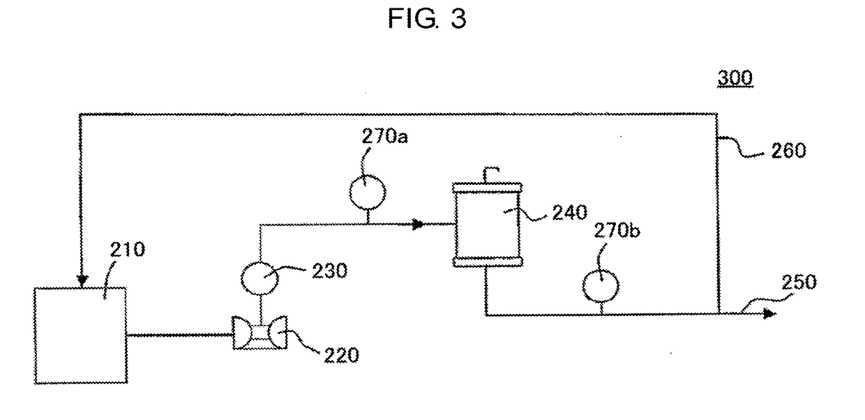
[0115]After the addition of 0.01 parts by mass of colloidal silica (“PL-1” manufactured by Fuso Chemical Co., Ltd., primary particle size: 15 nm) to 100 parts by mass of the composition, the mixture was filtered using the filtration device 300 illustrated in FIG. 3 (filtration step). The filtration device 300 illustrated in FIG. 3 includes a supply tank 210 that stores and supplies the composi...

example 24

4.3. Example 24

4.3.1. Preparation of Semiconductor Treatment Composition (Non-Dilution-Type Semiconductor Treatment Composition)

[0146]A polyethylene container was charged with each component listed in Table 3 in the ratio listed in Table 3. After the optional addition of potassium hydroxide and sodium hydroxide so that the pH, the K content, and the Na content listed in Table 3 were obtained, the mixture was stirred for 15 minutes.

[0147]The resulting semiconductor treatment composition (non-dilution-type semiconductor treatment composition) was filtered in the same manner as in Example 1, except that a filter in which a membrane-type cartridge filter “PE-CLEAN” (manufactured by Pall Corporation, nominal filtration rating: 0.05 micrometers, length: 10 inches) was provided in a housing, was used as the filter 240. The composition was sampled on a timely basis, and filtration was stopped when the number of particles having a particle size of 0.1 to 0.3 micrometers included in the semic...

example 25

4.4. Example 25

[0148]A semiconductor treatment composition (non-dilution-type semiconductor treatment composition) was prepared in the same manner as in Example 24, except that the composition was changed as listed in Table 3, and used directly as a treatment agent (resist stripper) as it is. Various evaluation tests were performed in the same manner as in Example 24.

4.5. Examples 26 to 29 and Comparative Examples 6 to 9

[0149]A semiconductor treatment composition (non-dilution-type semiconductor treatment composition) was prepared in the same manner as in Example 24, except that the composition was changed as listed in Table 3, and used directly as a treatment agent (etchant or resist stripper) without being diluted. Various evaluation tests were performed in the same manner as in Example 24.

4.6. Evaluation Results

[0150]The composition of each semiconductor treatment composition and the evaluation results are listed in Tables 1 to 3.

TABLE 1Example1234567SemiconductorCompound ATMAH0....


PUM


Abstract

A semiconductor treatment composition includes potassium, sodium, and a compound A represented by the formula (1), and has a potassium content MK (ppm) and a sodium content MNa (ppm) that satisfy MK/MNa=1×10−1 to 1×10⁴.

Description

[0001]Korean Patent Application No. 2017-0017335, filed on Feb. 8, 2017, is hereby incorporated by reference in its entirety.BACKGROUND OF THE INVENTION[0002]The present invention relates to a semiconductor treatment composition, and a treatment method that utilizes the semiconductor treatment composition.[0003]Chemical mechanical polishing (CMP) that is used to produce a semiconductor device is a technique that causes the processing target (polishing target) and a polishing pad to come in sliding contact with each other while pressing the processing target against the polishing pad, and supplying a chemical mechanical polishing aqueous dispersion (hereinafter may be referred to as “CMP slurry”) to the polishing pad to chemically and mechanically polish the processing target. The CMP slurry includes abrasive grains, and a chemical such as an etchant, and polishing waste (debris) is formed during CMP. A fatal device defect may occur if such polishing waste remains. Therefore, it is i...

Claims


Application Information

Patent Timeline
Patent Type & Authority Applications(United States)
IPC IPC(8): H01L21/321H01L21/306
CPCH01L21/3212B24B49/16B24B37/042H01L21/30625C09G1/02H01L21/02074H01L21/31133C09G1/00C09K3/14C11D3/02C11D3/2075C11D3/26C11D11/0047H01L21/02307H01L21/304H01L21/30604
Inventor HAYAMA, TAKAHIROKAMEI, YASUTAKANISHIGUCHI, NAOKIKAMO, SATOSHISHINODA, TOMOTAKA
Owner JSR CORPORATIOON
Why Eureka
Try Eureka