

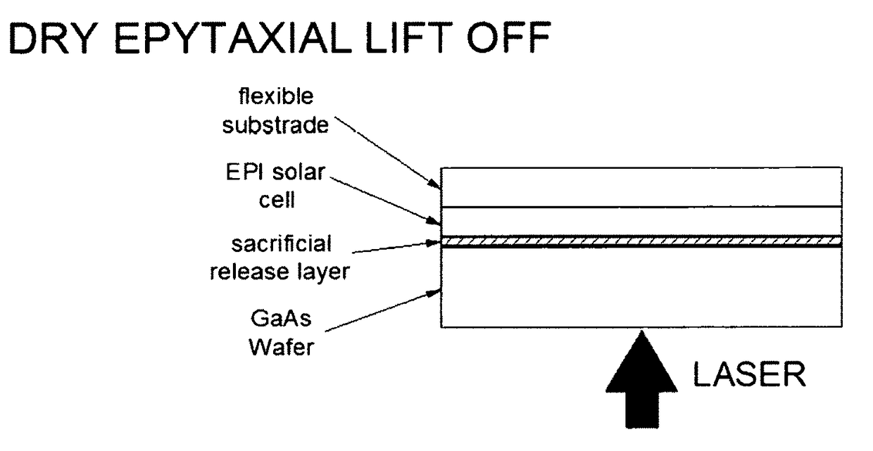
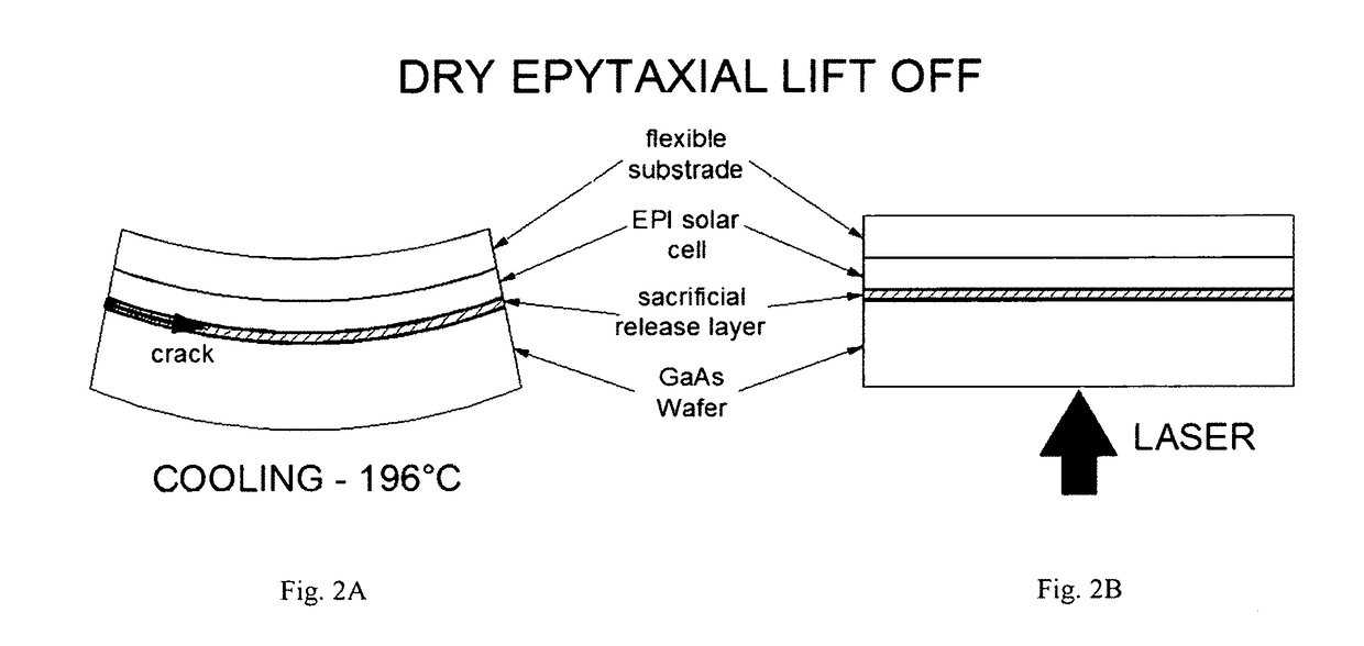
Laser epitaxial lift-off of high efficiency solar cell
- Summary
- Abstract
- Description
- Claims
- Application Information
AI Technical Summary
Benefits of technology
Problems solved by technology
Method used
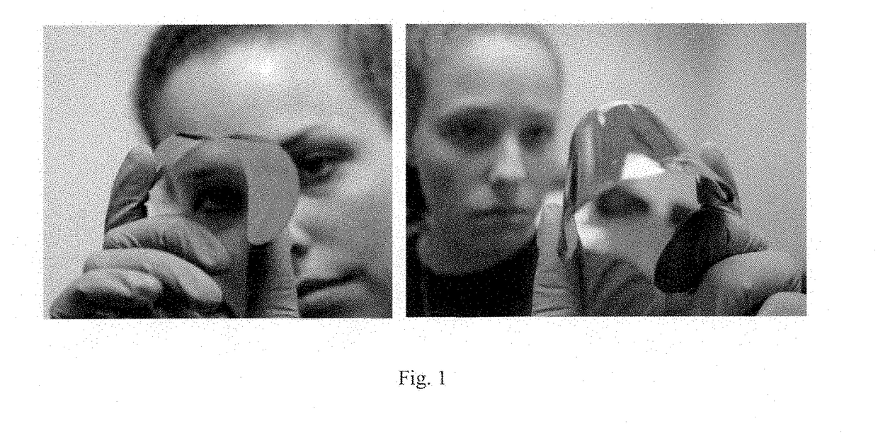
Image

Examples
example 1
nd Laser at 1.064 μm
[0106]The threshold of damage in Ge was observed at pulse energy of 2.4 mJ corresponding to an energy density of 300 mJ / cm2. The threshold of damage in GaAs was observed at pulse energy of 19.2 mJ corresponding to an energy density of 1.9 J / cm2. The data is shown in FIGS. 21A for Ge and 21B for GaAs. The ratio of the thresholds of GaAs / Ge is 6.33. Thus, Ge can be damaged with a margin of safety of 6.33 relative to GaAs. At this pulse energy (2.4 mJ), the damage in Ge was not visible after 10 pulses and was barely perceptible after 15 pulses. At this energy level, no damage could be seen in GaAs even after 6000 pulses.
example 2
nd Laser at 2.627 μm
[0107]FIG. 22A shows the damage in GaAs obtained with femtosecond laser at a fluence of 157 mJ / cm2 between 100 and 10000 pulses. FIG. 22B shows the same for Ge wafer. Under the same fluence and number of pulses GaAs damaged even more than Ge. The GaAs spot looks even darker than Ge after 500 shots. Even when the fluence was lowered to 137 mJ / cm2 and 127 mJ / cm2 GaAs remained darker than Ge after 1000 shots, as shown in FIGS. 23A and 23B. However, no damage was perceptible in either material below 120 mJ / cm2. The threshold of GaAs is lower than Ge at this wavelength and pulse width. This is due to the fact that 3PA for GaAs γI2=112,500 cm−1 while γI2=28,125 cm for Ge.
PUM
 Abstract
Description
Claims
Application Information