Method for inspecting ball grid array-type semiconductor chip package

a technology of semiconductor chips and grid arrays, applied in the direction of material analysis using wave/particle radiation, instruments, image enhancement, etc., can solve the problems of complex solventing process, difficult to inspect bga-type semiconductor chips for defects, and short circuits, etc., to achieve accurate acquisition of the region of interest, improve inspection reliability, and rapid inspection

Active Publication Date: 2019-07-25
KOREA ADVANCED INST OF SCI & TECH
View PDF0 Cites 5 Cited by
  • Summary
  • Abstract
  • Description
  • Claims
  • Application Information

AI Technical Summary

Benefits of technology

[0025]Recently, since information technology (IT) devices become small and are integrated, integrated semiconductor chips have three-dimensional (3D) structures extending from mainly two-dimensional (2D) substrates. According to the present invention, a ball grid array (BGA)-type semiconductor package having a 3D structure can be rapidly inspected. More specifically, the present invention can perform 3D image capturing once to obtain a reference image and can accurately obtain a region of interest using only a 2D image of a semiconductor chip. As a result, in a case in which a nondestructive inspection technique according to the present invention is applied to reliability inspection of a BGA-type semiconductor chip, a necessary time period can be significantly reduced as compared to that of a conventional 3D imaging technology (using computed tomography (CT) and laminography). In addition, since a cross section of interest obtained in conjunction with the 3D imaging technology does not overlap other cross sections, solder balls can be clearly checked, and thus reliability of inspection can also be improved. As described above, the present invention is a high-speed nondestructive radiation inspection technique suitable for an in-line inspection of a production site and can be actively applied to a system for inspecting for a defect in a process of manufacturing an information technology (IT) device, a device related to Internet of Things (IoT), and an automotive electric product.

Problems solved by technology

As the degree of integration of the PGA increases, intervals of the pins decrease, and thus a soldering process is complex, and there is a risk that a short circuit may occur.
However, there is a disadvantage in that it is very difficult to inspect the BGA-type semiconductor chip for defects.
When the BGA-type semiconductor package is attached to the printed circuit board, it is very difficult to inspect for soldering defects.
Although the inspection of the BGA may be overcome using an X-ray apparatus and a special microscope, a cost therefor is currently very high.
However, it is more difficult to inspect only a BGA layer disposed in one region of a semiconductor chip having a 3D structure in which a plurality of layers are stacked, that is, not a single layer, due to the development of the semiconductor chip technology as described above.
Since the solder balls of the BGA-type semiconductor chip with the 3D structure are hidden by elements of other integrated circuits or overlap solder balls of other layers, a solder ball array cannot be inspected using general image capturing.
Accordingly, it has been evaluated that an optical inspection technology is not suitable for inspecting the BGA-type semiconductor chip.
In addition, 2D X-ray inspection has a problem in that image quality of a target inspection region is highly degraded due to overlapping images of surrounding structures.
Referring to FIG. 1A, it is very difficult to obtain a cue for detecting a defect from a BGA image which is a region of interest and which is obtained from the image difference from the 2D projection image of the good product.
However, as illustrated in the drawing, a 2D imaging technique has disadvantages in that it is difficult to check features of solder balls, and a contrast degree thereof is low.
Particularly, since the solder balls positioned at an upper-right end overlap elements of other layers, it is very difficult to check accurate information on the solder balls.
Accordingly, a technology has been proposed for obtaining a partial 3D image using a laminography technology so as to obtain a higher quality image of a region of interest than that of a 2D image. FIG. 1B is an example of an image restored using the laminography, and although contrast degree is higher than that of the 2D image, it is still difficult to accurately distinguish other layers and resolution in a depth direction is low.
In addition, the method for inspecting with a 3D image using the laminography has problems in that 3D information may not be completely restored fundamentally, and an inspection time period may increase to a level which cannot be compared to that of the method for inspecting with a 2D image.
However, the prior patent has disadvantages in that a long time period for obtaining 2D projection images and restoring the images is needed as in laminography, and it is difficult to capture images of a chip having a large area with high resolution.
In order to produce high quality devices, inspection for defects is necessary during a manufacturing process, but, since a necessary time period of the 3D imaging inspection technology is much longer than that of the conventional 2D nondestructive inspection, productivity is reduced, and it is difficult to accurately analyze a BGA region of a highly integrated semiconductor chip using 2D imaging.

Method used


Image

  • Method for inspecting ball grid array-type semiconductor chip package
  • Method for inspecting ball grid array-type semiconductor chip package
  • Method for inspecting ball grid array-type semiconductor chip package

Examples


first embodiment

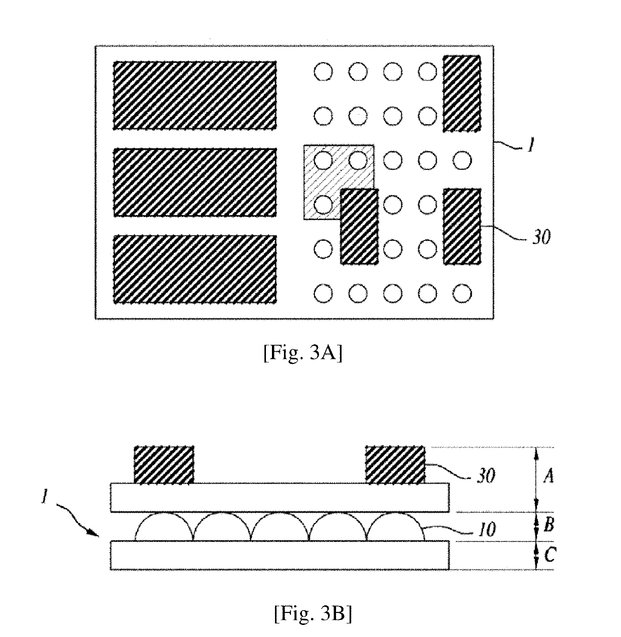
[0049]FIG. 2 is a flowchart illustrating a method for inspecting a BGA-type semiconductor chip package according to the present invention.

[0050]Referring to FIG. 2, the method for inspecting a BGA-type semiconductor chip package may include the steps of (a) capturing an image of a reference semiconductor chip (S101), (b) obtaining a reference image (S103), (c) capturing an image of a target semiconductor chip (S105), and (d) obtaining an image of a cross section of a BGA (S107).

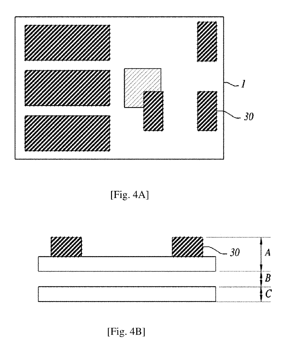
[0051]In the step (a) of S101, the 3D image of the reference semiconductor chip is obtained. The step (a) of S101 may be performed once or a plurality of times in an actual process so as to form a reference image.

[0052]In the step (a) of S101, the 3D image of any one reference semiconductor chip is captured using an X-ray computed tomography (CT). FIGS. 3A-3B are views illustrating a 3D image captured from a semiconductor chip 1 for obtaining a reference image in the method for inspecting from FIG. 2. FIG. 3A...

second embodiment

[0066]FIG. 6 is a flowchart illustrating a method for inspecting a BGA-type semiconductor chip package according to the present invention.

[0067]Referring to FIG. 6, the method for inspecting a BGA-type semiconductor chip package according to the second embodiment of the present invention may include the steps of (1) capturing a 3D image of a reference semiconductor chip (S201), (2) extracting an image of a BGA region (S203), (3) capturing a 2D image of the reference semiconductor chip (S205), (4) obtaining a reference image (S207), (5) capturing an image of a target semiconductor chip (S208), and (6) obtaining an image of a cross section of a BGA (S209).

[0068]In the step (1) of S201, the 3D image of the reference semiconductor chip may be obtained. In the step (1) of S201, the 3D image of any one reference semiconductor chip is captured using an X-ray CT. The step (1) of S201 corresponds to the above-described step (a) of S101, and an image of FIG. 3 may be obtained in the step (1) ...

third embodiment

[0077]FIG. 7 is a block diagram illustrating a configuration of an apparatus 100 for inspecting a semiconductor chip package according to the present invention. The apparatus 100 for inspecting a semiconductor chip package includes a first image acquisition unit 110, a second image acquisition unit 120, and an image processing unit 130.

[0078]The first image acquisition unit 110 uses a 3D image of a reference semiconductor chip to obtain a reference image in which a region of interest is removed from the 3D image.

[0079]The second image acquisition unit 120 obtains a 2D image of a target semiconductor chip.

[0080]The image processing unit 130 obtains an image of the region of interest from a difference between the reference image and the 2D image.

[0081]The reference semiconductor chip and the target semiconductor chip may include common regions of interest, such a region of interest may be preset, the image of the region of interest finally obtained by the image processing unit 130 may...


PUM

PropertyMeasurementUnit
specific angleaaaaaaaaaa
angleaaaaaaaaaa
nondestructive projection imaging techniqueaaaaaaaaaa

Abstract

Disclosed are a method, an apparatus, and a system for inspecting a ball grid array-type semiconductor chip package. A first embodiment of the present invention provides an apparatus for inspecting a semiconductor chip package, the apparatus comprising: a first image acquisition unit for acquiring a reference image using a three-dimensional image of a semiconductor chip serving as a reference, the reference image being obtained by removing a region of interest from the three-dimensional image; a second image acquisition unit for acquiring a two-dimensional image of a semiconductor chip to be inspected; and an image processing unit for deriving an image of a region of interest of the semiconductor chip to be inspected, from the difference between the reference image and the two-dimensional image.

Description

TECHNICAL FIELD[0001]The present invention relates to a method for inspecting a ball grid array (BGA)-type semiconductor chip package, and more particularly, to a method for inspecting a solder ball of a BGA-type semiconductor chip using a nondestructive projection imaging technique.BACKGROUND ART[0002]With the development of electronics and communication technologies, studies for small size and light weight of electronic devices are actively conducted. Due to this trend, a degree of integration of internal structure of a semiconductor chip necessarily increases. In order to minimize a problem in that a size of a semiconductor chip becomes large in a case in which the number of pins of an integrated circuit of the semiconductor chip is large, a semiconductor chip having a ball grid array (BGA) structure has been practically used. The BGA is derived from a pin grid array (PGA) in which pins are attached to a part or an entirety of one surface of a semiconductor chip in a grid shape. ...

Claims


Application Information

Patent Timeline
Patent Type & Authority Applications(United States)
IPC IPC(8): G01N21/95G06T7/00H04N13/20
CPCG01N21/951G06T2207/20104G01N21/9501G06T2207/30148G06T7/001H04N13/20G01N21/95684G01N2021/95646G01N23/046G01N2223/3306G01N2223/419G01N2223/611G06T2207/10028G01R31/2896G01N21/88G01R31/311G06T7/0004G06T11/00G06T7/00G01N23/18
Inventor CHO, SEUNGRYONGPARK, MIRANLEE, HOYEON
Owner KOREA ADVANCED INST OF SCI & TECH
Why Eureka
Try Eureka