Solid state thermochromic device, and method for producing said device

a thermochromic device and solid-state technology, applied in the direction of cosmonautic safety/emergency devices, cosmonautic parts, cosmonautic components, etc., can solve the problems of liquid electrolytes presenting a risk of leakage and/or irreversible deformation, devices presenting a risk of interface delamination,

Active Publication Date: 2019-08-08
COMMISSARIAT A LENERGIE ATOMIQUE ET AUX ENERGIES ALTERNATIVES +1
View PDF0 Cites 6 Cited by
  • Summary
  • Abstract
  • Description
  • Claims
  • Application Information

AI Technical Summary

Benefits of technology

[0049]The term “infrared-reflective layer b)”, is understood to mean that this layer is always reflective in the range of mid infrared (IR), namely for wavelengths of 2.5 to 25 μm, and that it is also, possibly, preferably, reflective in the near IR of 0.78 to 2.5 μm, as this contributes to reducing solar absorptivity: it is, in particular, the case of a layer of silver with a thickness of 100 nm, but not of metal oxide layers because they are not sufficiently conductive.
[0156]In fact, in order to fluidize the method and reduce the overall cost, it is advantageous to produce the device continuously, under vacuum, and without the need to open the machine.

Problems solved by technology

Such devices present a risk of delamination of the interfaces, particularly on the front face, unless a complex preparation and activation process is implemented.
However, organic electrochromic devices remain difficult to adapt to spatial conditions for the thermal protection of satellites, because the polymers are sensitive to extreme temperatures and to UV, while the liquid electrolytes present a risk of leakage and / or of irreversible deformation when put under a high (secondary) vacuum.
Inorganic electrochromic devices are more resistant than their organic counterparts, but their integration still requires the implementation of electrical contacts and a voltage control management system, because their emissivity varies with their redox potential through electrochemical activation.
The essential disadvantage of the solid state thermochromic devices of the prior art described above lies in the fact that the SiO2 and HfO2 dielectric layers have phonons bands between 9 and 16 μm which generate strong absorptions that may reduce the performances of the devices.

Method used


Image

  • Solid state thermochromic device, and method for producing said device
  • Solid state thermochromic device, and method for producing said device
  • Solid state thermochromic device, and method for producing said device

Examples


example

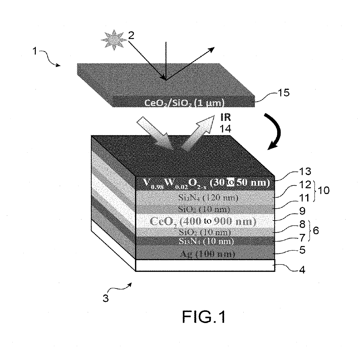
[0264]All the layers of the device according to the invention, and prepared by the device according to the invention, are prepared by implementing the same technique, namely the magnetron cathode sputtering technique, in the same magnetron sputtering chamber under vacuum (namely, at a residual pressure lower than 10−6 mbar (high vacumm, secondary vacuum) before introduction of the plasma-forming gases that are used during the deposition phases of the materials in thin layers which are carried out under primary vacuum (rough vacuum)), under a pressure of argon, or of a mixture of argon and nitrogen, or of a mixture of argon and oxygen in reactive mode, while maintaining the vacuum between the deposition of two successive layers and without opening the chamber before the last layer of the device is deposited.

[0265]A different target must however be used for the deposition of each layer containing a different metal. Thus, the interface layers use the same target (Si), while the solar p...


PUM

PropertyMeasurementUnit
temperatureaaaaaaaaaa
thicknessaaaaaaaaaa
thicknessaaaaaaaaaa

Abstract

A solid-state thermochromic device and method for producing the device, the device including: a stack successively including, from a rear face to a front face exposed to solar radiation: a) a solid substrate of an inorganic material resistant up to a temperature of 550° C.; b) an infrared-reflective layer of an electronically conductive material; c) electronically insulating interface layers; d) an electronically insulating inorganic dielectric layer transparent to infrared radiation, of cerium oxide CeO2, with a thickness between 400 and 900 nm; e) electronically insulating interface layers; f) a layer of an infrared-active thermochromic material, an n-doped VO2 vanadium oxide, and crystallized in a monoclinic or rutile phase, with a thickness between 30 and 50 nm; and g) a solar-protective coating, transparent to infrared radiation.

Description

TECHNICAL AREA[0001]The invention relates to a solid-state (all-solid) thermochromic device.[0002]More specifically, the invention relates to a solid-state (all-solid) thermochromic device that is active in the infrared, and refers to any solid state comprising an inorganic stack of thin layers with a layer of a thermochromic material based on vanadium oxide IV, VO2.[0003]More precisely still, the device according to the invention is a solid state thermochromic device with emissivity that may be modulated in the infrared (IR) and with low solar absorptivity.[0004]The term “solid-state device” (“all-solid device”) is understood to mean a device consisting solely of inorganic materials that are solid at room temperature.[0005]The invention further relates to a method for producing said device.[0006]The technical field of the invention may, in general, be defined as that of so-called “solid state” (all-solid) devices active in the infrared, operating in the infrared, or infrared operat...

Claims


Application Information

Patent Timeline
Patent Type & Authority Applications(United States)
IPC IPC(8): G02B5/08B64G1/22B64G1/58C03C17/36
CPCG02B5/0858B64G1/226B64G1/58C03C17/3626C03C17/3644C09K9/00G02B7/008C03C17/36C03C17/3681
Inventor MARCEL, CORINNESABARY, FREDERICVERDALET GUARDIOLA, XAVIERREMAURY, STEPHANIE
Owner COMMISSARIAT A LENERGIE ATOMIQUE ET AUX ENERGIES ALTERNATIVES
Why Eureka
Try Eureka