
Light-emitting layer for perovskite light-emitting device, method for manufacturing same, and perovskite light-emitting device using same

a technology of light-emitting devices and light-emitting layers, which is applied in the direction of organic semiconductor devices, luminescent compositions, lead halides, etc., can solve the problems of difficult uniform control of the size of the quantum dots, the wide spectrum of existing organic light-emitters, and the intrinsic limitations of organic light-emitters and inorganic quantum dots light-emitters, etc., to achieve the effect of improving the luminescent efficiency and luminance of the devi

Active Publication Date: 2019-08-22
SN DISPLAY CO LTD
View PDF3 Cites 6 Cited by
  • Summary
  • Abstract
  • Description
  • Claims
  • Application Information

AI Technical Summary

Benefits of technology

The patent describes a method for manufacturing a light emitting device using organic-inorganic-hybrid perovskite or inorganic metal halide perovskite. The device has a high color purity and the light emitting layer can be introduced to improve its efficiency and luminance. The method involves combining the FCC and BCC crystal structures, which results in the formation of nanocrystal particles with a lamellar structure where the organic and inorganic planes are alternately stacked. Excitons are confined in the inorganic plane, which enhances the device's color purity. The manufacturing process involves synthesizing the perovskite nanoparticles and then introducing them into the light emitting layer to improve the device's efficiency and luminance.

Problems solved by technology

However, in the viewpoint of emitting materials, both the organic light-emitters and the inorganic quantum dot light-emitters have intrinsic limitations.
The existing organic light-emitter have an advantage of high efficiency, but the existing organic light-emitter have a wide spectrum and poor color purity.
Although the inorganic quantum dot light-emitter have been known to have good color purity because the luminescence occurs by quantum size effects, there is a problem that it is difficult to uniformly control the sizes of the quantum dots as the color approaches the blue color, and thereby the size distribution deteriorate the color purity.
Also, both light-emitters (organic emitters and inorganic quantum dot emitters) are disadvantageously expensive.
Therefore, the organic-inorganic-hybrid perovskite incorporating the emitting organic ammonium are unsuitable for a light emitting layer.
Thus, in this case, it is not very suitable for the light-emitter having the high color purity, which is highlighted in this patent.
However, since the organic-inorganic-hybrid perovskite has small exciton binding energy, there is a fundamental problem that the luminescence occurs at a low temperature, but the excitons do not emit light at room temperature due to thermal ionization and delocalization of a charge carrier and thus are easily separated as free charge carriers and then annihilated.
Also, there is a problem in that the excitons are annihilated by the layer having high conductivity in the vicinity of the excitons after the free charge carriers are recombined again to form excitons.

Method used


Image

  • Light-emitting layer for perovskite light-emitting device, method for manufacturing same, and perovskite light-emitting device using same
  • Light-emitting layer for perovskite light-emitting device, method for manufacturing same, and perovskite light-emitting device using same
  • Light-emitting layer for perovskite light-emitting device, method for manufacturing same, and perovskite light-emitting device using same

Examples


manufacturing example 1

Manufacture of Solution Including Organic-Inorganic-Hybrid Perovskite Colloidal Nanoparticle

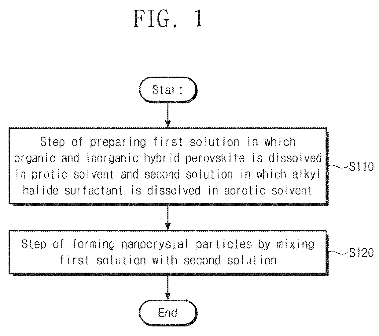
[0270]A solution including an organic-inorganic-hybrid perovskite colloidal nanoparticle including an organic-inorganic-hybrid perovskite nanocrystal structure according to an embodiment of the present invention was formed. The colloidal solution was formed through an inverse nano-emulsion method, or reprecipitation method, or hot injection method.

[0271]Particularly, organic-inorganic-hybrid perovskite was dissolved in a polar solvent to prepare a first solution. Here, dimethylformamide was used as the polar solvent, and (CH3NH3)2PbBr4 was used as the organic-inorganic-hybrid perovskite. Here, the used (CH3NH3)2PbBr4 was prepared by mixing CH3NH3Br with PbBr2 at a ratio of 2:1.

[0272]Also, a second solution in which an alkyl halide surfactant is dissolved in a non-polar solvent was prepared. Here, toluene was used as the non-polar solvent, and octadecylammonium bromide (CH3(CH2)17NH3Br) was us...

manufacturing example 2

Manufacture of Light Emitting Layer

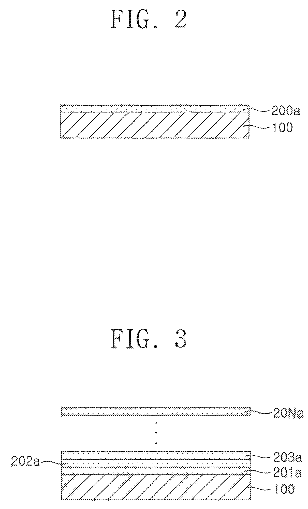
[0274]First, a 10 wt % 3-mercaptopropionic acid (MPA, Aldrich) ethanolic solution was spin-coated on a glass substrate to form an anchoring agent layer. After the excess MPA is removed through washing using ethanol and chloroform, the perovskite nanocrystal manufactured by Manufacturing Example 1 was spin-coated on the anchoring agent layer to form a perovskite nanocrystal layer (2500 rpm and 20 s).

[0275]The perovskite nanocrystal that is not anchored through the chloroform spin-costing (2500 rpm and 20 s) was removed. To adjust a thickness of the perovskite nanocrystal layer, spin-coating (2500 rpm and 20 s) of a 1 wt % 1,2-ethanedithiol (EDT) / ethanol solution having 250 μL and spin-coating (2500 rpm and 20 s) of the perovskite nanocrystal solution was spin-coated (2500 rpm and 20 s) were repeatedly performed to form the light emitting device.

manufacturing example 3

Manufacture of Light Emitting Layer

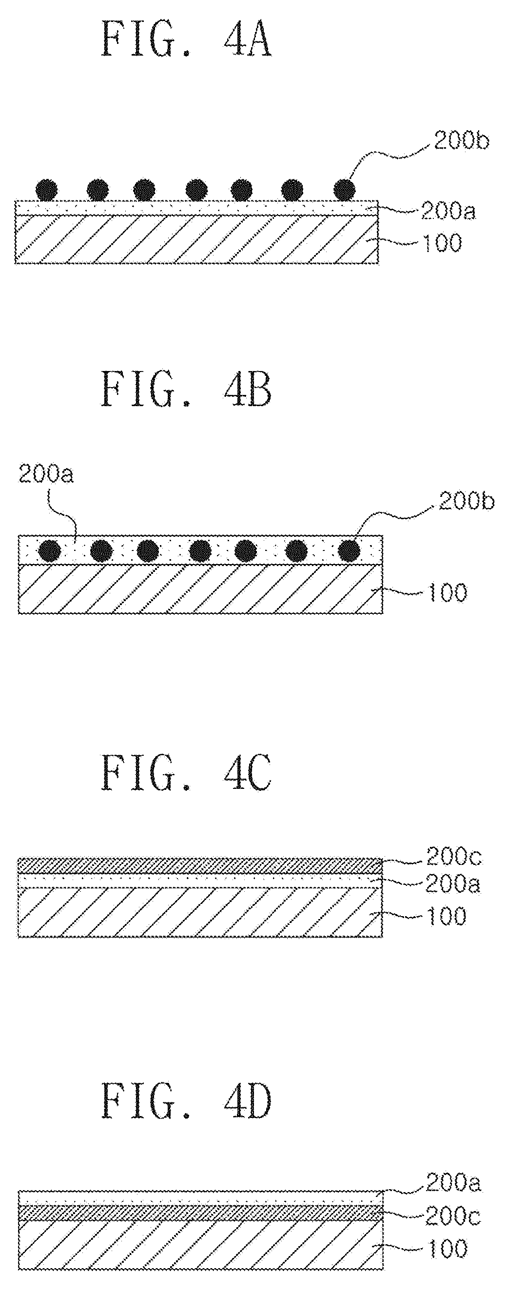
[0276]First, a trioctylphosphine oxide (TOPO) solution and a trioctylphosphine (TOP) solution was added to the perovskite nanocrystal solution manufactured by Embodiment 1 to substitute a ligand of the perovskite nanocrystal with TOPO and TOP. Then, N,N′-diphenyl,N′-bis(3-methylphenyl)-(1,1′-biphenyl)-4,4′-diamine(TPD) was mixed with the perovskite nanocrystal solution at a ratio of 100:5 (w / w) to manufacture a TPD-perovskite nanocrystal solution. The TPD-perovskite nanocrystal solution was spin-coated (500 rpm 7 s, 3000 rpm, and 90 s) to form a TPD and perovskite nanocrystal layer. Here, the TPD and perovskite nanocrystal was phase-separated while the spin-coating to form a nano thin film including the organic-inorganic-hybrid perovskite nanoparticle including the perovskite nanocrystal structure on the TPD layer.


PUM

PropertyMeasurementUnit
full width at half maximumaaaaaaaaaa
sizeaaaaaaaaaa
surface energyaaaaaaaaaa

Abstract

Provided are: a light-emitting layer for a perovskite light-emitting device; a method for manufacturing the same; and a perovskite light-emitting device using the same. The method of the present invention for manufacturing a light-emitting layer for an organic and inorganic hybrid perovskite light-emitting device comprises a step of forming a first nanoparticle thin film by coating, on a member for coating a light-emitting layer, a solution comprising organic and inorganic perovskite nanoparticles including an organic and inorganic perovskite nanocrystalline structure. Thereby, a nanoparticle light emitter has therein an organic and inorganic hybrid perovskite having a crystalline structure in which FCC and BCC are combined; forms a lamella structure in which an organic plane and an inorganic plane are alternatively stacked; and can show high color purity since excitons are confined to the inorganic plane. In addition, it is possible to improve the luminescence efficiency and luminance of a device by making perovskite as nanoparticles and then introducing the same into a light-emitting layer.

Description

TECHNICAL FIELD[0001]The present invention relates to light-emitters and their light emitting device, and more particularly, to a light emitting layer for an organic-inorganic-hybrid perovskite or inorganic metal halide perovskite light emitting device, a method for manufacturing the same, a light emitting device using the same, and a method for manufacturing the light emitting device.BACKGROUND ART[0002]The megatrend of the display market is shifting from the existing high-efficiency and high-resolution-oriented display, to the emotional image-quality display aiming at realizing a high color purity for demonstration of natural colors. In this respect, organic light-emitter-based organic light emitting diode (OLED) devices using organic light-emitters have remarkably developed, inorganic quantum dot LEDs with the improved color purity have been actively researched and developed as alternatives. However, in the viewpoint of emitting materials, both the organic light-emitters and the ...

Claims


Application Information

Patent Timeline
Patent Type & Authority Applications(United States)
IPC IPC(8): H01L51/00C09K11/06C01G21/16C09K11/66H01L31/0352C09K11/02C07F7/24H01L31/032H01L51/50H01L31/00
CPCH01L51/0077C09K11/06C01G21/16C09K11/665H01L31/0352C09K11/025C07F7/24H01L31/032H01L51/0034H01L51/0037H01L51/004H01L51/0072H01L51/502H01L31/00H01L51/5206H01L51/5096H01L51/442H01L51/4273H01L51/426H01L51/0003C01P2004/64C01P2002/60C01P2002/34B82Y30/00H01L2251/308C01P2006/40B82Y20/00B82Y40/00C09K2211/10C09K2211/188H01L51/0059Y10S977/774Y10S977/788Y10S977/813Y10S977/892Y10S977/896Y10S977/948Y10S977/95C09K11/664Y02E10/549H10K71/15H10K85/631H10K50/115H10K85/50H10K85/30H10K85/10H10K85/141H10K85/1135H10K85/6572H10K30/35H10K30/82H10K30/353H10K50/18H10K50/81H10K71/12H10K2102/103
Inventor LEE, TAE-WOOIM, SANGHYUKCHO, HIMCHANKIM, YOUNG-HOON
Owner SN DISPLAY CO LTD
Learn More