
Light-emitting layer for perovskite light-emitting device, method for manufacturing same, and perovskite light-emitting device using same

a technology of light-emitting devices and light-emitting layers, which is applied in the direction of organic semiconductor devices, luminescent compositions, lead halides, etc., can solve the problems of difficult uniform control of the size of the quantum dots, the wide spectrum of existing organic light-emitters, and the intrinsic limitations of organic light-emitters and inorganic quantum dots light-emitters, etc., to achieve the effect of improving the luminescent efficiency and luminance of the devi

Active Publication Date: 2019-04-30
SN DISPLAY CO LTD
View PDF10 Cites 3 Cited by
  • Summary
  • Abstract
  • Description
  • Claims
  • Application Information

AI Technical Summary

Benefits of technology

The patent is about a method for making a perovskite light emitting device using organic-inorganic-hybrid perovskite or inorganic metal halide. The device has a crystal structure with both FCC and BCC structures combined, which results in high color purity. The device also has a lamellar structure, where organic and inorganic layers alternate, which improves the luminescent efficiency and luminance of the device. Additionally, the patent describes an introduction of a light emitting layer to further enhance the device's performance. Overall, the patent provides technical means to create high-quality perovskite light emitting devices with improved efficiency and luminosity.

Problems solved by technology

However, in the viewpoint of emitting materials, both the organic light-emitters and the inorganic quantum dot light-emitters have intrinsic limitations.
The existing organic light-emitter have an advantage of high efficiency, but the existing organic light-emitter have a wide spectrum and poor color purity.
Although the colloidal inorganic quantum dot light-emitter have been known to high good color purity because the luminescence occurs by quantum size effects, there is a problem that it is difficult to uniformly control the sizes of the quantum dots as the color approaches the blue color, and thereby the size distribution deteriorate the color purity because of size distribution.
Also, both light-emitters (organic emitters and colloidal inorganic quantum dot emitters) are disadvantageously expensive.
Therefore, the organic-inorganic-hybrid perovskite incorporating the emitting organic ammonium are unsuitable for a light emitting layer.
Thus, in this case, it is not very suitable for the light-emitter having the high color purity, which is highlighted in this patent.
However, because the organic-inorganic-hybrid perovskite has small exciton binding energy, there is a fundamental problem that the luminescence occurs at a low temperature, but the excitons do not emit light at room temperature due to thermal ionization and delocalization of a charge carrier and thus are easily separated as free charge carriers and then annihilated.
Also, there is a problem in that the excitons are annihilated by the layer having high conductivity in the vicinity of the excitons after the free charge carriers are recombined again to form excitons.

Method used


Image

  • Light-emitting layer for perovskite light-emitting device, method for manufacturing same, and perovskite light-emitting device using same
  • Light-emitting layer for perovskite light-emitting device, method for manufacturing same, and perovskite light-emitting device using same
  • Light-emitting layer for perovskite light-emitting device, method for manufacturing same, and perovskite light-emitting device using same

Examples


example 2

Manufacturing Manufacture of Light Emitting Layer

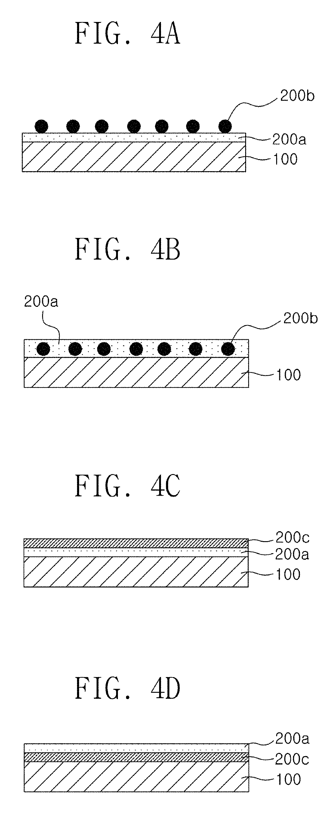
[0291]First, a 10 wt % 3-mercaptopropionic acid (MPA, Aldrich) ethanolic solution was spin-coated on a glass substrate to form an anchoring agent layer. After the excess MPA is removed through washing using ethanol and chloroform, the perovskite nanocrystal manufactured by Manufacturing Example 1 was spin-coated on the anchoring agent layer to form a perovskite nanocrystal layer (2500 rpm and 20 s).

[0292]The perovskite nanocrystal that is not anchored through the chloroform spin-costing (2500 rpm and 20 s) was removed. To adjust a thickness of the perovskite nanocrystal layer, spin-coating (2500 rpm and 20 s) of a 1 wt % 1,2-ethanedithiol (EDT) / ethanol solution having 250 μL and spin-coating (2500 rpm and 20 s) of the perovskite nanocrystal solution was spin-coated (2500 rpm and 20 s) were repeatedly performed to form the light emitting device.

example 3

Manufacturing Manufacture of Light Emitting Layer

[0293]First, a trioctylphosphine oxide (TOPO) solution and a trioctylphosphine (TOP) solution was added to the perovskite nanocrystal solution manufactured by Embodiment 1 to substitute a ligand of the perovskite nanocrystal with TOPO and TOP. Then, N,N′-diphenyl,N′-bis(3-methylphenyl)-(1,1′-biphenyl)-4,4′-diamine(TPD) was mixed with the perovskite nanocrystal solution at a ratio of 100:5 (w / w) to manufacture a TPD-perovskite nanocrystal solution. The TPD-perovskite nanocrystal solution was spin-coated (500 rpm 7 s, 3000 rpm, and 90 s) to form a TPD and perovskite nanocrystal layer. Here, the TPD and perovskite nanocrystal was phase-separated while the spin-coating to form a nano thin film including the organic-inorganic-hybrid perovskite nanoparticle including the perovskite nanocrystal structure on the TPD layer.

example 4

Manufacturing Manufacture of Light Emitting Layer

[0294]First, a Si native wafer was dipped into a octadecyltrichlorosilane (ODTS) solution to manufacture an ODTS-treated wafer. Also, a perovskite nanocrystal was spin-coated (1500 rpm and 60 s) on the ODTS-treated wafer to form a perovskite nanocrystal layer. Polydimethylsiloxane (PDMS) was poured on a flat silicon wafer and cured at a temperature of 75° C. for 2 hours to manufacture a PDMS stamp. The PDMS stamp was completely closely attached to the perovskite nanocrystal layer to apply a sufficient pressure, and then rapidly remove the stamp, thereby separating the perovskite nanocrystal from the ODTS-treated wafer. The separated perovskite nanocrystal was separated from the PDMS through contact with a previously prepared indium tin oxide (ITO) / PEDOT:PSS substrate.


PUM

PropertyMeasurementUnit
thicknessaaaaaaaaaa
surface roughnessaaaaaaaaaa
full width at half maximumaaaaaaaaaa

Abstract

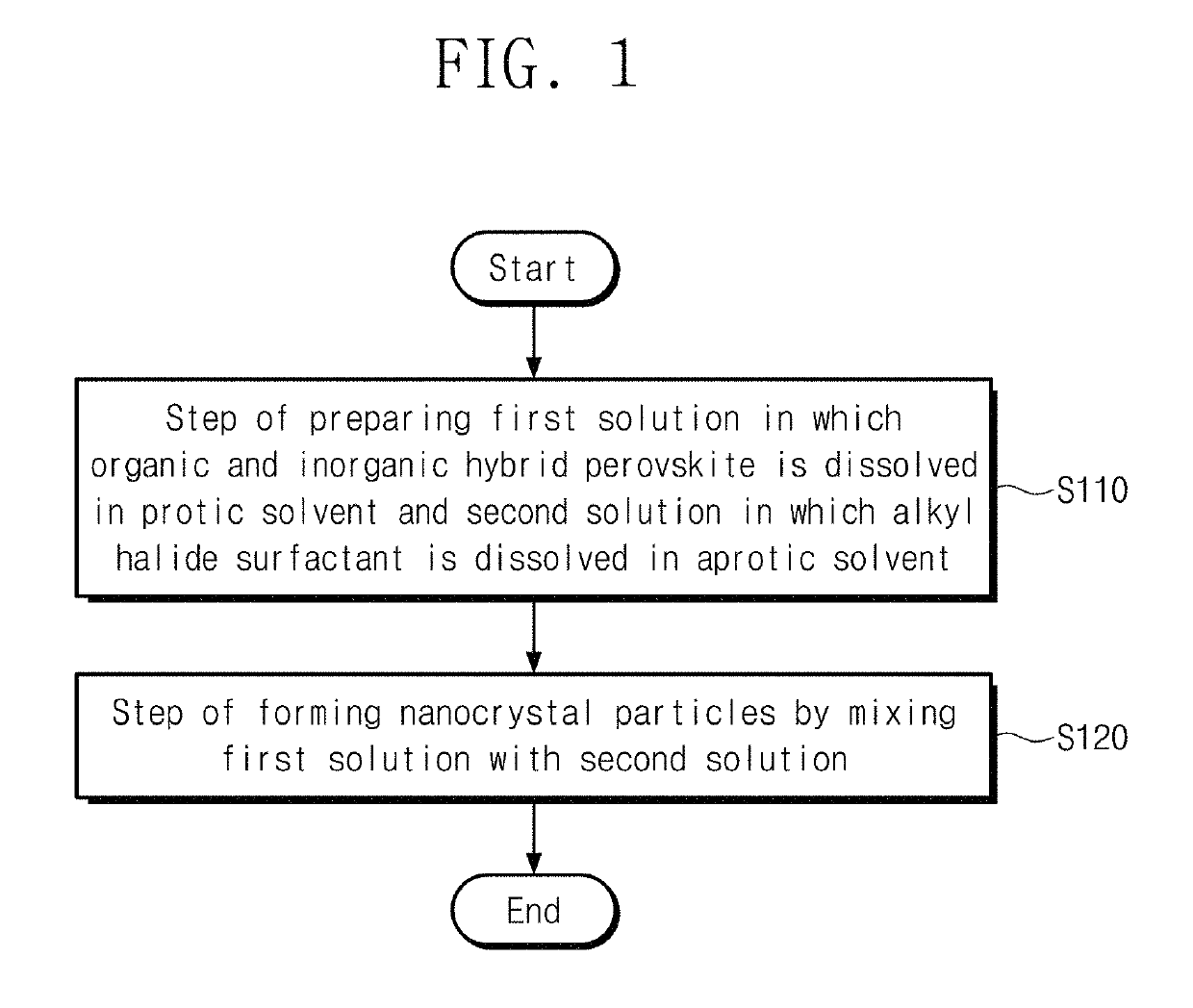
Disclosed are a light-emitting layer for a perovskite light-emitting device, a method for manufacturing the same, and a perovskite light-emitting device using the same. The method of manufacturing the light-emitting layer comprises a step of forming a first nanoparticle thin film by coating, on a substrate for coating a light-emitting layer, a solution comprising organic and inorganic perovskite nanoparticles. Thereby, a nanoparticle light emitter has therein an organic and inorganic hybrid perovskite having a crystalline structure in which FCC and BCC are combined, and has a lamella structure in which an organic plane and an inorganic plane are alternatively stacked. Also, high color purity is realized because excitons are confined to the inorganic plane.

Description

TECHNICAL FIELD[0001]The present invention relates to light-emitters and their light emitting device, and more particularly, to a light emitting layer for an organic-inorganic-hybrid perovskite or inorganic metal halide perovskite light emitting device, a method for manufacturing the same, a light emitting device using the same, and a method for manufacturing the light emitting device.BACKGROUND ART[0002]The major trend of the display market is shifting from the existing high-efficiency and high-resolution-oriented display, to the emotional image-quality display aiming at realizing a high color purity for demonstration of natural colors. From this viewpoint, organic light-emitter-based organic light emitting diode (OLED) devices using organic light-emitters have remarkably developed, inorganic quantum dot LEDs with the improved color purity have been actively researched and developed as alternatives. However, in the viewpoint of emitting materials, both the organic light-emitters an...

Claims


Application Information

Patent Timeline
Patent Type & Authority Patents(United States)
IPC IPC(8): H01L31/00H01L51/50C09K11/06C01G21/16B82Y40/00C09K11/66C07F7/24C09K11/02H01L51/00H01L51/42B82Y30/00B82Y20/00H01L51/44H01L51/52H10K99/00
CPCH01L51/0077C07F7/24C09K11/025C09K11/06C09K11/665H01L31/00H01L51/004H01L51/0034H01L51/0037H01L51/0072H01L51/502C01G21/16Y10S977/95B82Y20/00B82Y30/00B82Y40/00C01P2002/34C01P2002/60C01P2004/64C01P2006/40C09K2211/10C09K2211/188H01L51/0003H01L51/0059H01L51/426H01L51/4273H01L51/442H01L51/5096H01L51/5206H01L2251/308Y10S977/774Y10S977/788Y10S977/813Y10S977/892Y10S977/896Y10S977/948H01L31/032H01L31/0352C09K11/664Y02E10/549H10K71/15H10K85/631H10K50/115H10K85/50H10K85/30H10K85/10H10K85/141H10K85/1135H10K85/6572H10K30/35H10K30/82H10K30/353H10K50/18H10K50/81H10K71/12H10K2102/103
Inventor LEE, TAE-WOOIM, SANGHYUKCHO, HIMCHANKIM, YOUNG-HOON
Owner SN DISPLAY CO LTD
Learn More