Light-emitting layer for perovskite light-emitting device, method for manufacturing same, and perovskite light-emitting device using same
- Summary
- Abstract
- Description
- Claims
- Application Information
AI Technical Summary
Benefits of technology
Problems solved by technology
Method used
Image
Examples
example 2
Manufacturing Manufacture of Light Emitting Layer
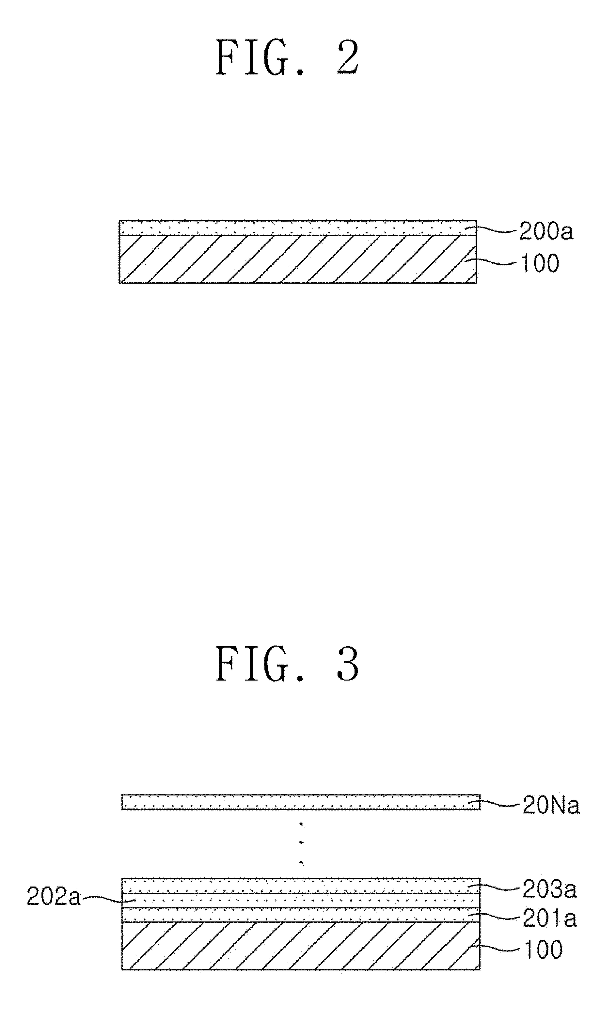
[0274]First, a 10 wt % 3-mercaptopropionic acid (MPA, Aldrich) ethanolic solution was spin-coated on a glass substrate to form an anchoring agent layer. After the excess MPA is removed through washing using ethanol and chloroform, the perovskite nanocrystal manufactured by Manufacturing Example 1 was spin-coated on the anchoring agent layer to form a perovskite nanocrystal layer (2500 rpm and 20 s).
[0275]The perovskite nanocrystal that is not anchored through the chloroform spin-costing (2500 rpm and 20 s) was removed. To adjust a thickness of the perovskite nanocrystal layer, spin-coating (2500 rpm and 20 s) of a 1 wt % 1,2-ethanedithiol (EDT) / ethanol solution having 250 μL and spin-coating (2500 rpm and 20 s) of the perovskite nanocrystal solution was spin-coated (2500 rpm and 20 s) were repeatedly performed to form the light emitting device.
example 3
Manufacturing Manufacture of Light Emitting Layer
[0276]First, a trioctylphosphine oxide (TOPO) solution and a trioctylphosphine (TOP) solution was added to the perovskite nanocrystal solution manufactured by Embodiment 1 to substitute a ligand of the perovskite nanocrystal with TOPO and TOP. Then, N,N′-diphenyl,N′-bis(3-methylphenyl)-(1,1′-biphenyl)-4,4′-diamine(TPD) was mixed with the perovskite nanocrystal solution at a ratio of 100:5 (w / w) to manufacture a TPD-perovskite nanocrystal solution. The TPD-perovskite nanocrystal solution was spin-coated (500 rpm 7 s, 3000 rpm, and 90 s) to form a TPD and perovskite nanocrystal layer. Here, the TPD and perovskite nanocrystal was phase-separated while the spin-coating to form a nano thin film including the organic-inorganic-hybrid perovskite nanoparticle including the perovskite nanocrystal structure on the TPD layer.
example 4
Manufacturing Manufacture of Light Emitting Layer
[0277]First, a Si native wafer was dipped into a octadecyltrichlorosilane (ODTS) solution to manufacture an ODTS-treated wafer. Also, a perovskite nanocrystal was spin-coated (1500 rpm and 60 s) on the ODTS-treated wafer to form a perovskite nanocrystal layer. Polydimethylsiloxane (PDMS) was poured on a flat silicon wafer and cured at a temperature of 75° C. for 2 hours to manufacture a PDMS stamp. The PDMS stamp was completely closely attached to the perovskite nanocrystal layer to apply a sufficient pressure, and then rapidly remove the stamp, thereby separating the perovskite nanocrystal from the ODTS-treated wafer. The separated perovskite nanocrystal was separated from the PDMS through contact with a previously prepared indium tin oxide (ITO) / PEDOT:PSS substrate.
PUM
| Property | Measurement | Unit |
|---|---|---|
| Thickness | aaaaa | aaaaa |
| Thickness | aaaaa | aaaaa |
| Surface roughness | aaaaa | aaaaa |
Abstract
Description
Claims
Application Information


