
Microwave transmission apparatus and semiconductor processing device

Active Publication Date: 2019-08-29
BEIJING NAURA MICROELECTRONICS EQUIP CO LTD
View PDF3 Cites 36 Cited by
  • Summary
  • Abstract
  • Description
  • Claims
  • Application Information

AI Technical Summary

Benefits of technology

The present disclosure provides improvements for a microwave transmission apparatus and a semiconductor processing device to increase the frequency range and expand the scenarios where they can be used.

Problems solved by technology

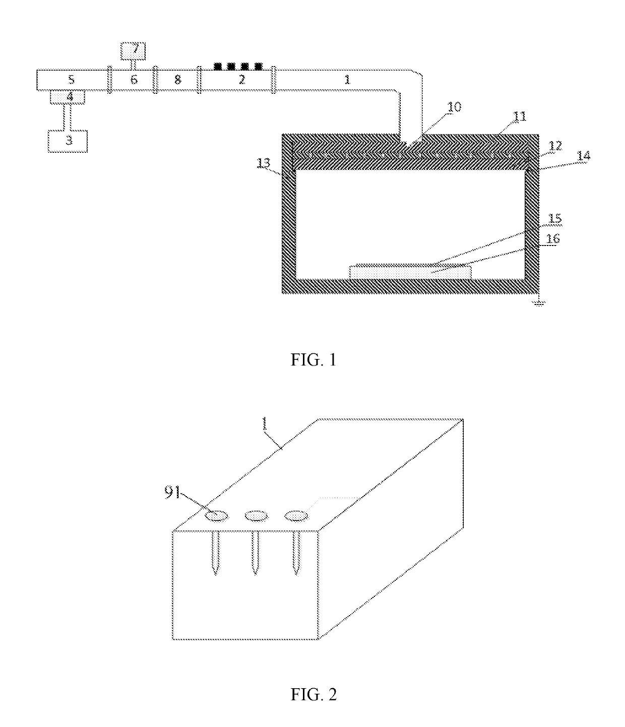
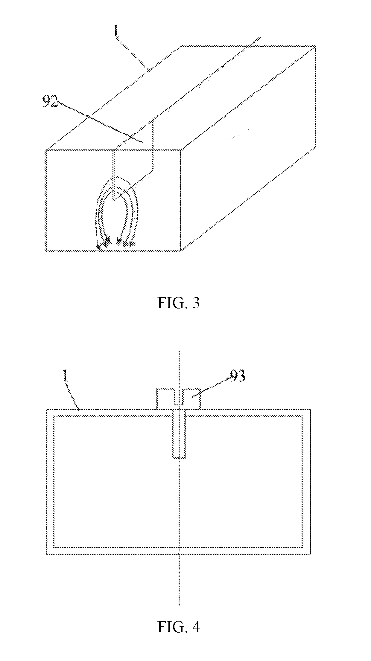
However, the equivalent capacitor and the equivalent inductor formed in the waveguide 1 by the metal pin or the metal diaphragm as an impedance matching structure have fixed values, and thus can only be used as single reactance-fixed elements.
Therefore, the metal pin or the metal diaphragm can only be used for impedance matching for a fixed load or a load with small variations, and it is difficult to adapt to impedance matching under load changes.
However, because the short side length of the waveguide 1 is fixed, which limits the adjustable range of the length of the screw 93 into the inside of the waveguide 1.
Therefore, the impedance matching range of the impedance matching structure described above is small, which limits the applicable operating frequency range and the applicable scenarios of the microwave transmission apparatus.

Method used


Image

  • Microwave transmission apparatus and semiconductor processing device
  • Microwave transmission apparatus and semiconductor processing device
  • Microwave transmission apparatus and semiconductor processing device

Examples


Embodiment Construction

[0057]Reference will now be made in detail to exemplary embodiments of the disclosure, which are illustrated in the accompanying drawings. Wherever possible, the same reference numbers will be used throughout the drawings to refer to the same or like parts.

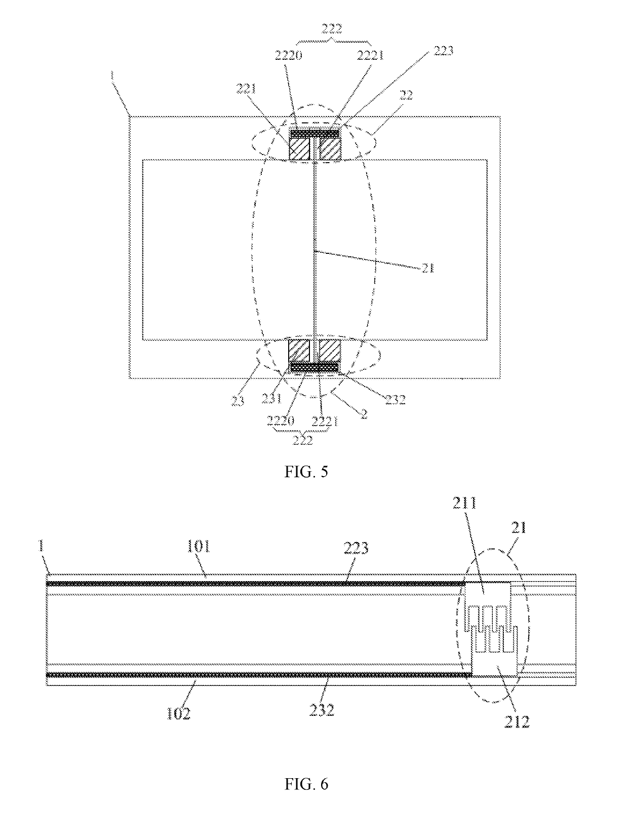
[0058]The present disclosure provides a microwave transmission apparatus. FIGS. 5 and 6 illustrate schematic cross-sectional views of an exemplary microwave transmission apparatus consistent with various embodiments of the present disclosure. Specifically, FIG. 5 illustrates a schematic cross-sectional view of the microwave transmission apparatus along a direction perpendicular to the extending direction of the waveguide, and FIG. 6 illustrates a schematic cross-sectional view of the microwave transmission apparatus along a direction parallel to an extending direction of the waveguide.

[0059]Referring to FIGS. 5 and 6, the microwave transmission apparatus may include a waveguide 1 and an impedance matching structure 2 disposed in t...


PUM


Abstract

The present disclosure provides a microwave transmission apparatus. The microwave transmission apparatus includes a waveguide, configured to transmit microwaves emitted from a microwave source to a load; and an impedance matching structure, disposed in the waveguide the waveguide. The waveguide includes a microstrip interdigital capacitor. The impedance before the input end of the impedance matching structure is matched with the impedance after the input end of the impedance matching structure by adjusting an equivalent capacitance formed by the microstrip interdigital capacitor and / or a position of the microstrip interdigital capacitor along the extending direction of the waveguide.

Description

CROSS-REFERENCES TO RELATED APPLICATIONS[0001]This application is a continuation application of International Application No. PCT / CN2017 / 088979, filed on Jun. 19, 2017, which claims the priority and benefits of Chinese Patent Application Serial No. CN201611013118.3, filed with the State Intellectual Property Office of P. R. China on Nov. 15, 2016, the entire content of all of which is incorporated herein by reference.FIELD OF THE DISCLOSURE[0002]The present disclosure relates to the field of semiconductor device processing technology and, more particularly, relates to a microwave transmission apparatus and a semiconductor processing device.BACKGROUND[0003]Conventional semiconductor fabrication processes have used plasma processing devices in various types, such as the capacitively coupled plasma (CCP) type, the inductively coupled plasma (ICP) type, and the surface wave or electron cyclotron resonance (ECR) plasma type, etc. Among them, the surface wave plasma does not need to incre...

Claims


Application Information

Patent Timeline
IPC IPC(8): H01J37/32H01P3/08H03H7/38
CPCH01J37/32229H03H7/383H01P3/081H01J37/32311H01J37/32211H01L21/67011H01P3/12H01P5/024H01J37/32H01L21/67
Inventor LIU, CHUNMING
Owner BEIJING NAURA MICROELECTRONICS EQUIP CO LTD
Learn More