Electronic component and method of producing electronic component

a technology of electronic components and components, applied in the direction of semiconductor/solid-state device details, fixed capacitor details, printed circuit non-printed electric components association, etc., can solve the problems of affecting connection reliability, affecting the flatness of the board, and affecting the volume occupied by the chip capacitor, so as to reduce the coefficient of linear thermal expansion and reduce the cost. , the effect of preventing dimensional variation

Active Publication Date: 2019-08-29
TOPPAN PRINTING CO LTD
View PDF0 Cites 8 Cited by
  • Summary
  • Abstract
  • Description
  • Claims
  • Application Information

AI Technical Summary

Benefits of technology

[0010]The present invention has been made in light of the circumstances set forth above and aims to provide a miniaturized and thin electronic component having improved or even high reliability by using a board that has a thin film capacitor of a MIM structure having improved or even high reliability, and a method of producing an electronic component.
[0016]According to the present invention, a glass core base is used as a core board. The glass core base has low coefficient of linear thermal expansion and high coefficient of elasticity, and thus can prevent dimensional variation due to thermal cycling, and can ensure connection reliability of the electronic circuit and the external connection terminals during thermal cycling. Furthermore, the ends of the upper electrode are ensured to be separated from the respective ends of the lower electrode, and the upper and lower electrodes are electrically isolated from each other by the dielectric layer. Thus, a short circuit is better prevented from occurring between the electrodes, and electrical reliability is enhanced.

Problems solved by technology

Specifically, increase in volume occupied by a chip capacitor involves limitation to routing of wires.
Moreover, if an inorganic core is used, flatness of the board may be impaired due to the embedded chip capacitor.
In addition, such boards having built-in capacitors may impair connection reliability due to the difference in coefficient of linear thermal expansion between the organic board and the chip component.
When forming a capacitor of a MIM (metal insulator metal) structure in a multilayer circuit using an organic core board, a short circuit or an open failure may occur in the capacitor, deteriorating reliability.

Method used


Image

  • Electronic component and method of producing electronic component
  • Electronic component and method of producing electronic component
  • Electronic component and method of producing electronic component

Examples


example 1

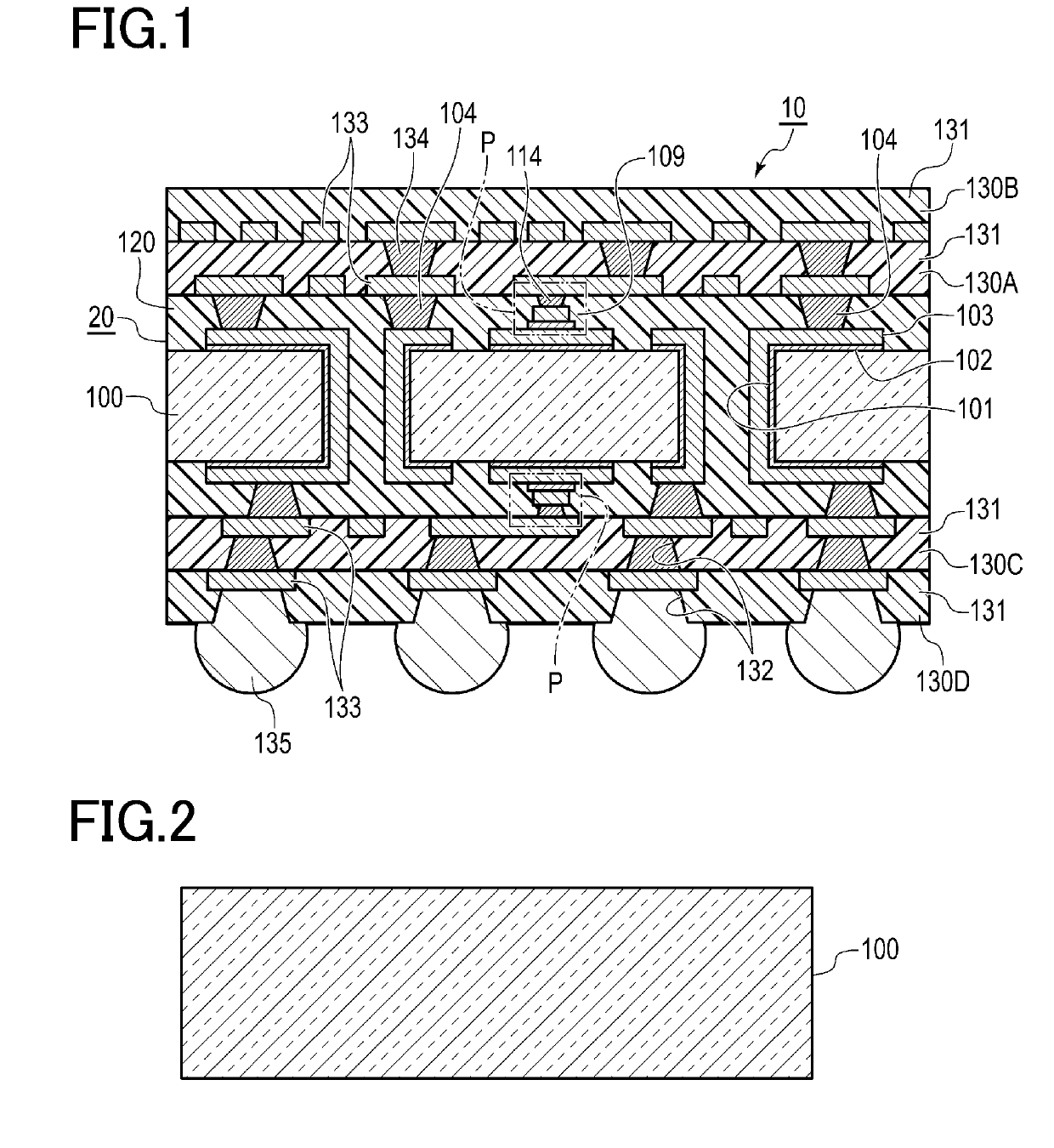
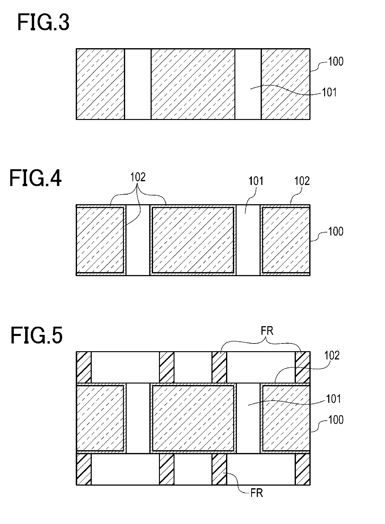
[0086]A glass base 100 (OA-10G with a thickness of 0.5 mm and a coefficient of linear thermal expansion of 3 ppm / K, manufactured by Nippon Electric Glass Co., Ltd.) as shown in FIG. 2 was used. Subsequently, as shown in FIG. 3, through holes 101 were formed with a top diameter of 80 μm and a bottom diameter of 60 μm by using a picosecond laser beam machine. Then, as shown in FIG. 4, a titanium film with a thickness of 50 nm and a copper film with a thickness of 300 nm were formed by sputtering on the front and back surfaces of the glass base 100 so as to serve as a seed metal layer 102. Then, an electroless nickel layer was formed with a thickness of 0.1 μm to increase the thickness of the seed metal layer 102 in the respective through holes 101. Thus, a seed metal layer 102 of titanium, copper and nickel was formed.

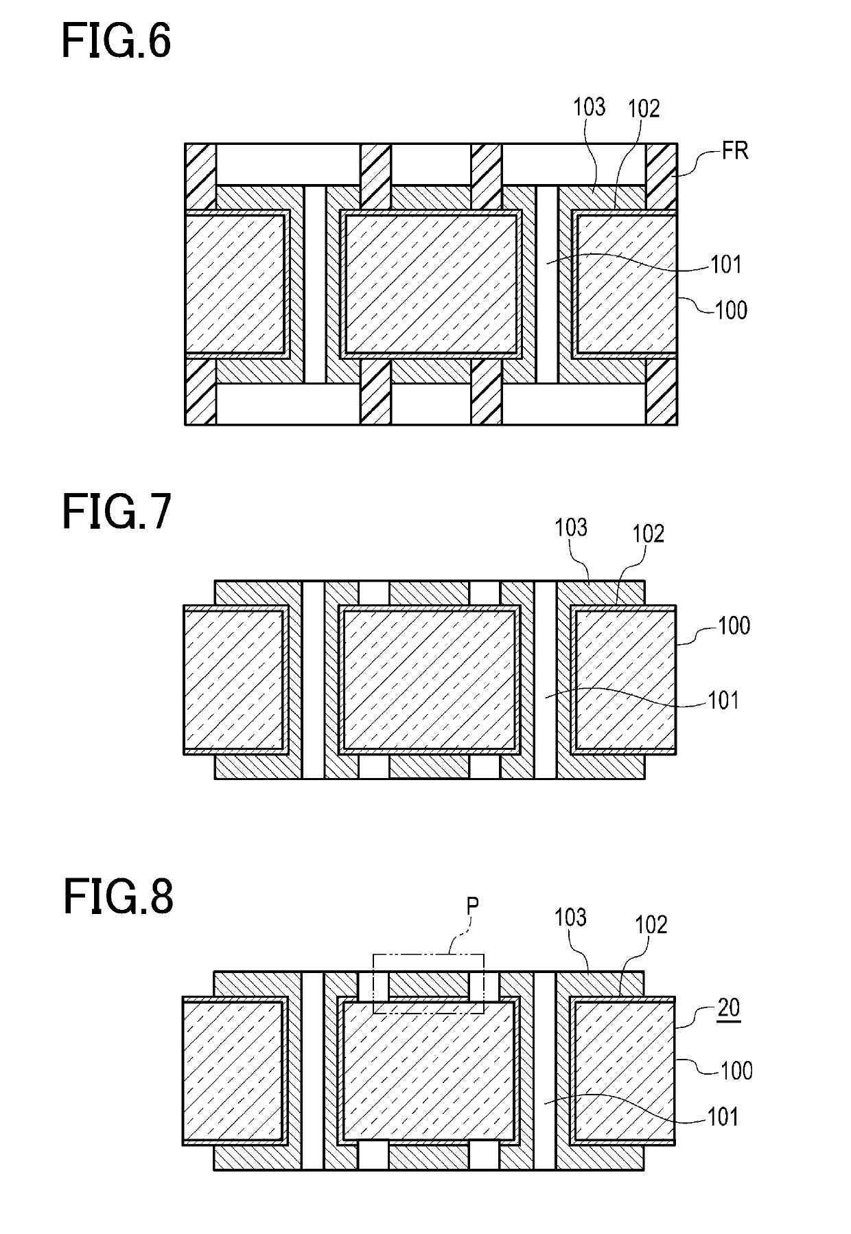
[0087]Then, as shown in FIG. 5, a photosensitive dry film resist with a thickness of 25 μm was provided onto the seed metal layer 102 by roll lamination, and a resist pa...


PUM

PropertyMeasurementUnit
thicknessaaaaaaaaaa
thicknessaaaaaaaaaa
diameteraaaaaaaaaa

Abstract

An electronic component includes a glass base in which through holes are formed passing through both surfaces thereof; an insulating resin layer laminated on each of both surfaces of the glass base and including a copper plated layer formed therein; and a capacitor including a lower electrode formed on the copper plated layer, a dielectric layer laminated on the lower electrode, and an upper electrode laminated on the dielectric layer. In the electronic component, the upper electrode has a region that is parallel to the copper plated layer and is formed so as to be smaller than a region of the dielectric layer parallel to the surface of the copper plated layer or a region of the lower electrode parallel to the surface of the copper plated layer.

Description

CROSS-REFERENCE TO RELATED PATENT APPLICATIONS[0001]This application is a continuation application filed under 35 U.S.C. § 111(a) claiming the benefit under 35 U.S.C. §§ 120 and 365(c) of International Patent Application No. PCT / JP2017 / 043339, filed on Dec. 1, 2017, which is based upon and claims the benefit of priority to Japanese Patent Application No. 2016-235277, filed on Dec. 2, 2016; the disclosures of which are all incorporated herein by reference in their entireties.TECHNICAL FIELD[0002]The present invention relates to an electronic component and a method of producing an electronic component, and in particular relates to an electronic component incorporating a capacitor that has a structure less likely to cause a short circuit and ensuring high reliability.BACKGROUND ART[0003]In recent years, following the trend of achieving high performance and miniaturization in electronic devices, there are growing needs of developing high-density circuit boards configuring semiconductor ...

Claims


Application Information

Patent Timeline
Patent Type & Authority Applications(United States)
IPC IPC(8): H05K1/16H01G4/228H01G4/33H01L23/15H05K3/46H05K3/38H01G4/06
CPCH05K1/162H01G4/228H01G4/33H05K3/46H05K3/38H01L23/15H01G4/06H01G4/38H01G4/12H01G4/236H01G4/248H01L23/49822H01L23/49827H05K3/4605H05K1/0271H05K2201/068H05K2201/10378H01L2924/15311H01L2924/19105H01L2224/16237H01L23/12H05K1/16H05K1/0231H05K1/18H05K1/111
Inventor TAKAGI, FUSAONAKAMURA, KIYOTOMO
Owner TOPPAN PRINTING CO LTD
Why Eureka
Try Eureka