LAYERED GaAs, METHOD OF PREPARING SAME, AND GaAs NANOSHEET EXFOLIATED FROM SAME

a nanosheet and gallium arsenide technology, applied in the field of layered gallium arsenide (gaas), can solve the problems of high limit in research on 2d materials, limited possibility of low-dimensional material development, and high cost, and achieve easy exfoliation into nanosheets, excellent electrical properties, and easy charge transport

Inactive Publication Date: 2019-11-21
IND ACADEMIC CORP FOUND YONSEI UNIV
View PDF0 Cites 8 Cited by
  • Summary
  • Abstract
  • Description
  • Claims
  • Application Information

AI Technical Summary

Benefits of technology

[0007]The present invention is directed to providing: layered GaAs, which, unlike conventional bulk GaAs, has a 2D crystal structure, has the ability to be easily exfoliated into nanosheets, and exhibits excellent electrical properties by having a structure that enables easy charge transport in the in-plane direction; and a GaAs nanosheet exfoliated from the same.

Problems solved by technology

In particular, the top-down method always requires that the pristine form of a target subject to be exfoliated have a 2D layered crystal structure, and thus researchable subjects thereof are highly limited to graphene without band gap, layered metal oxides / nitrides with low charge mobility, transition metal chalcogen compounds with low electron mobility / low electrical conductivity, and the like.
Due to limitations of the existing research methods, research on 2D materials has been highly limited to materials such as graphene, transition metal chalcogen compounds, and the like.
Such existing research methods have limitations in that the possibility of low-dimensional material development is limited, in essence, by the types of elements to be used, and the methods are not suitable for use in the development of low-dimensional future materials out of the myriad of three-dimensional (3D) bulk-type materials not having a layered structure.

Method used


Image

  • LAYERED GaAs, METHOD OF PREPARING SAME, AND GaAs NANOSHEET EXFOLIATED FROM SAME
  • LAYERED GaAs, METHOD OF PREPARING SAME, AND GaAs NANOSHEET EXFOLIATED FROM SAME
  • LAYERED GaAs, METHOD OF PREPARING SAME, AND GaAs NANOSHEET EXFOLIATED FROM SAME

Examples


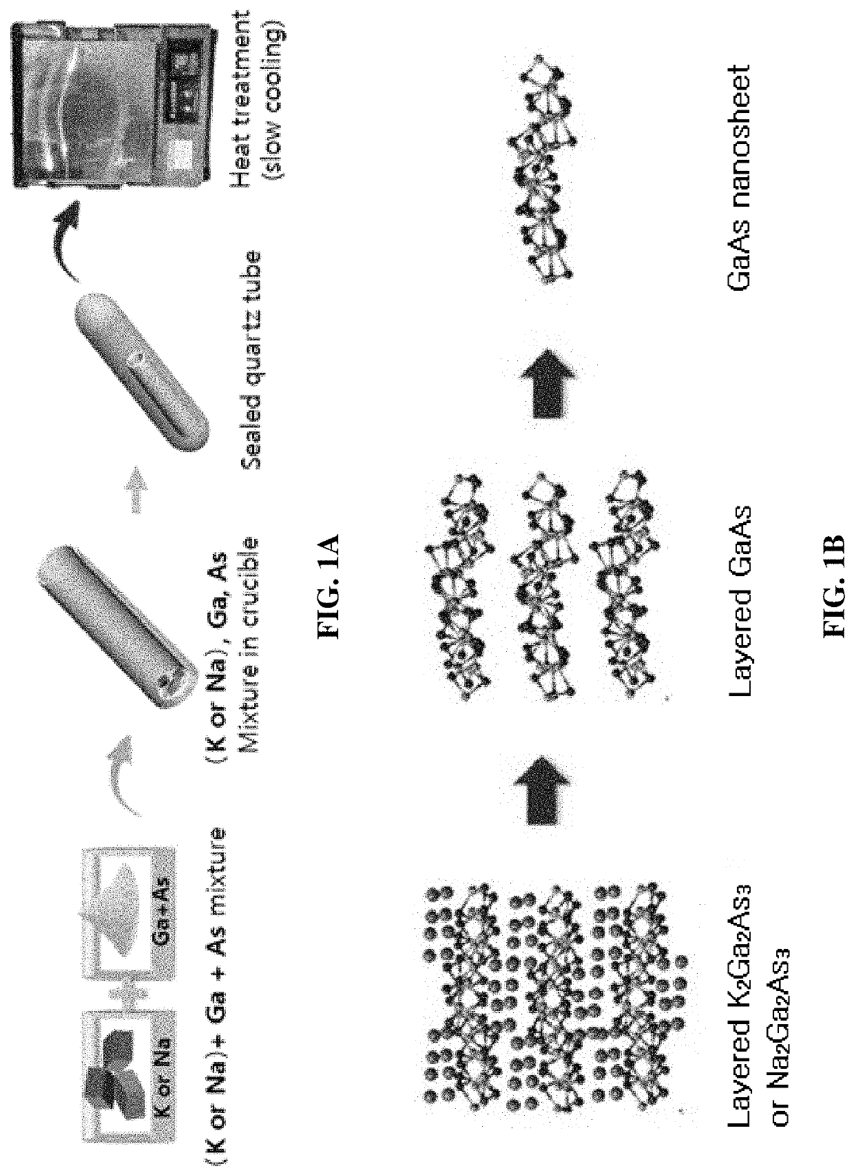
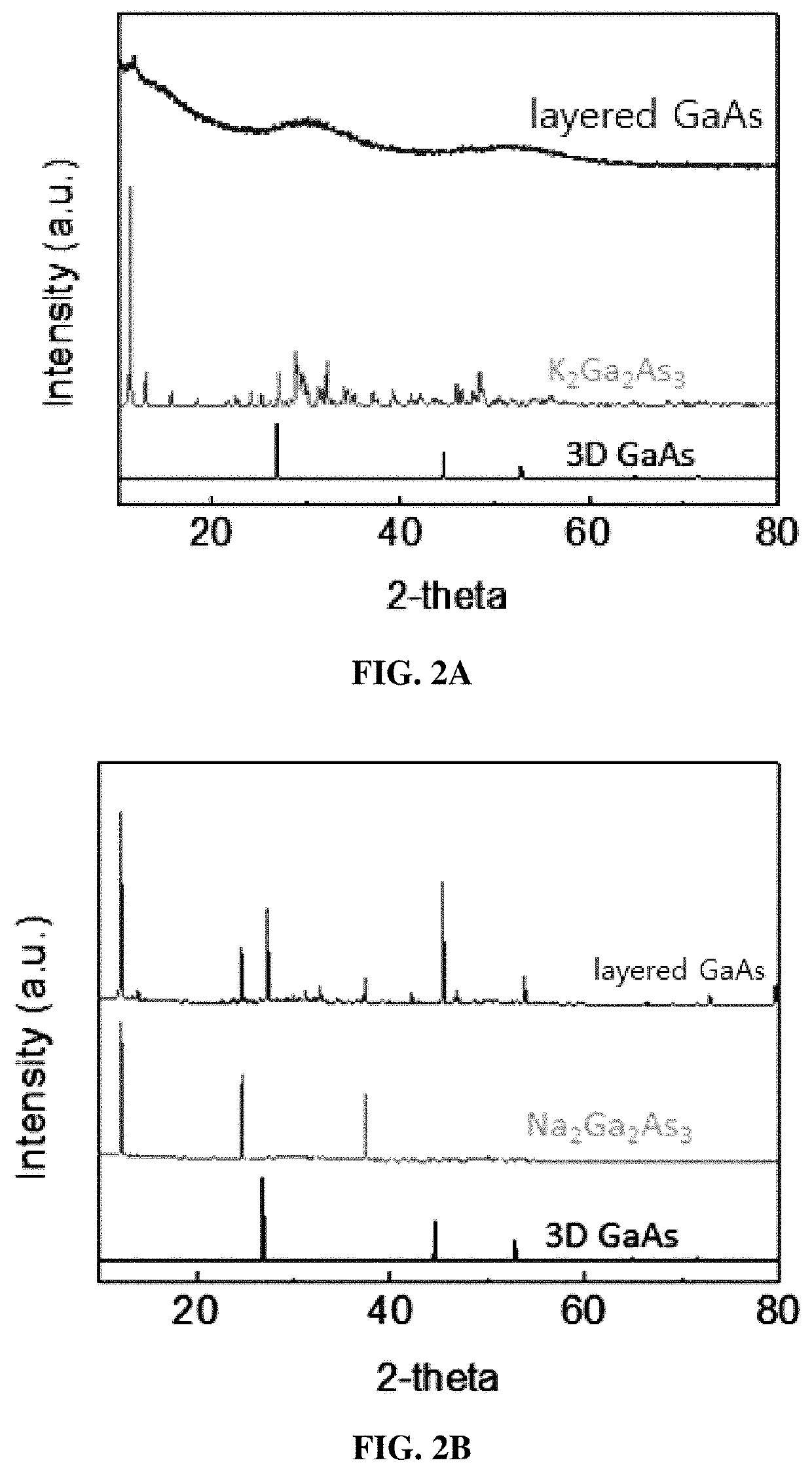
preparation example 1

Preparation of Layered K2Ga2As3

[0074]A predetermined amount of K powder was mixed with a predetermined amount of Ga powder and As powder, and the mixtxure was sealed in a quart tube in an inert gas atmosphere. The quartz tube containing the sample was heat-treated for 10 hours at 750° C. Afterwards, the tube was cooled at a cooling rate of 0.5 to 3° C. / hr for K2Ga2As3 recrystallization, thereby obtaining a K2Ga2As3 single crystal having a monoclinic crystal structure with the P21 / c space group.

preparation example 2

Preparation of Layered Na2Ga2As3

[0075]A predetermined amount of Na powder was mixed with a predetermined amount of Ga powder and As powder, and the mixture was sealed in a quartz tube in an inert gas atmosphere. The quartz tube containing the sample was heat-treated for 10 hours at 750° C. Afterwards, the tube was cooled at a cooling rate of 1° C. / hr for Na2Ga2As3 recrystallization, thereby obtaining a Na2Ga2As3 single crystal having a monoclinic crystal structure with the P21 / c space group.

example 1

Preparation of Layered GaAs

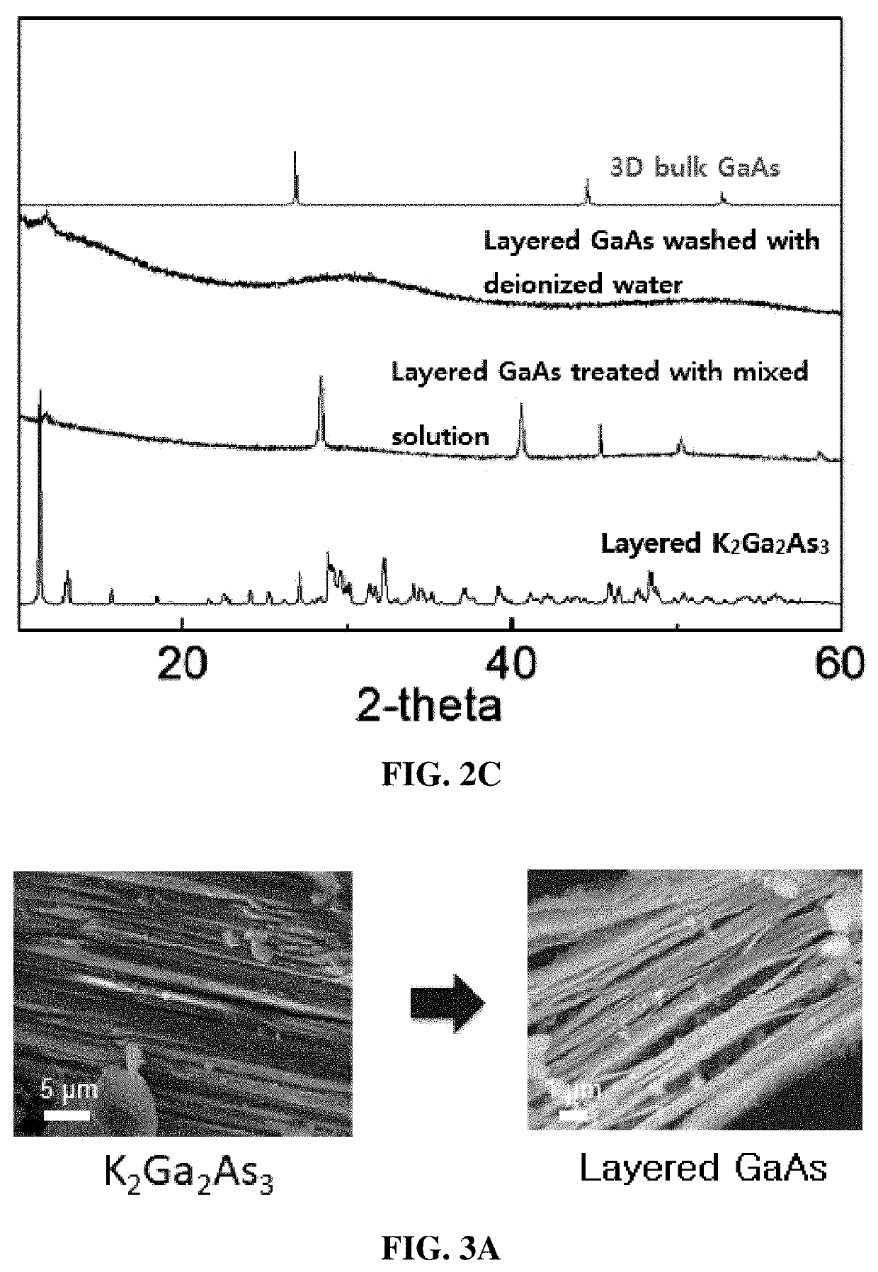
[0076]The K2Ga2As3 prepared in Preparation Example 1 was mixed with deionized water, ethanol, and AlCl3 to remove K ions therefrom, and after washed with deionized water to remove KCl, layered GaAs having an amorphous structure was obtained.


PUM

PropertyMeasurementUnit
thicknessaaaaaaaaaa
temperatureaaaaaaaaaa

Abstract

The present invention relates to: layered gallium arsenide (GaAs), which is more particularly layered GaAs, which, unlike the conventional bulk GaAs, has a two-dimensional crystal structure, has the ability to be easily exfoliated into nanosheets, and exhibits excellent electrical properties by having a structure that enables easy charge transport in the in-plane direction; a method of preparing the same; and a GaAs nanosheet exfoliated from the same.

Description

CROSS-REFERENCE TO RELATED APPLICATION[0001]This application claims priority to and the benefit of Korean Patent Application No. 2018-0057449, filed on May 18, 2018, the disclosure of which is incorporated herein by reference in its entirety.BACKGROUND1. Field of the Invention[0002]The present invention relates to layered gallium arsenide (GaAs), a method of preparing the same, and a GaAs nanosheet exfoliated from the same. More particularly, the present invention relates to: layered GaAs, which, unlike conventional bulk GaAs, has a two-dimensional (2D) crystal structure, has the ability to be easily exfoliated into nanosheets, and exhibits excellent electrical properties by having a structure that enables easy charge transport in an in-plane direction; a method of preparing the same; and a GaAs nanosheet exfoliated from the same.2. Discussion of Related Art[0003]Research on graphene and various other ultra-thin 2D materials based on the novel physical, chemical, mechanical, and opt...

Claims


Application Information

Patent Timeline
Patent Type & Authority Applications(United States)
IPC IPC(8): C30B29/42C30B11/00C30B29/68H01L29/20H01L29/06H01L21/02
CPCH01L29/20C30B29/68C30B29/42C30B11/003H01L29/0665H01L21/02546H01L21/02623C01G28/00B82Y40/00C01P2002/72C01P2004/20C01P2004/03C01P2004/04C01P2002/85C01P2002/82C01P2004/02H01L21/0259H01L29/2003B82Y30/00C01G28/002C01P2002/76C01P2002/20C01P2002/02C30B29/60C30B11/00C30B33/08
Inventor SHIM, WOO YOUNGCHOI, SANG JINKIM, HYESOO
Owner IND ACADEMIC CORP FOUND YONSEI UNIV
Why Eureka
Try Eureka