Double-sided electrode structure and patterning process thereof

a technology of double-sided electrodes and electrodes, applied in the direction of printed circuit aspects, instruments, electric digital data processing, etc., can solve the problems of high cost, complex manufacturing process, low yield, many problems to be solved, etc., and achieve the effect of high manufacturing efficiency

Active Publication Date: 2019-12-05
CAMBRIOS FILM SOLUTIONS CORP
View PDF0 Cites 16 Cited by
  • Summary
  • Abstract
  • Description
  • Claims
  • Application Information

AI Technical Summary

Benefits of technology

[0009]Some embodiments of this disclosure provide a patterning method of a double-

Problems solved by technology

However, this laser patterning method applied to the metal oxide thin film has the problems of high cost, complex manufacturing processes, and low yield.
When utilizing nanowires to manufacture touch electrodes, there are many issues to be solved in the manufacturing process and structure of the metal wiring of the nanowires and the peripheral area.
However, the above-mentioned manufacturing method defines the upper electrode structure and the lower electrode structure in different processes, so that manufacturing steps are complex and require more manufacturing time.
When utilizing laser technology to perform the patterning process on the nanowir

Method used


Image

  • Double-sided electrode structure and patterning process thereof
  • Double-sided electrode structure and patterning process thereof
  • Double-sided electrode structure and patterning process thereof

Examples


Embodiment Construction

[0038]The various embodiments of the present disclosure are illustrated in the drawings, and the practical details will be described in the following embodiments. However, it should be understood that these practical details are not intended to limit the disclosure. That is, in some embodiments of the disclosure, these practical details are not necessary. In addition, some of the conventional structures and elements are shown in the drawings in a simplified manner.

[0039]As used herein, “about” or “rough” is generally an error or a range within 20% of a value, preferably a range within 10%, and more preferably a range within 5%. Unless otherwise stated, the numerical values mentioned in this disclosure are considered as approximations, that is, they have an error or a range as indicated by “about” or “rough”.

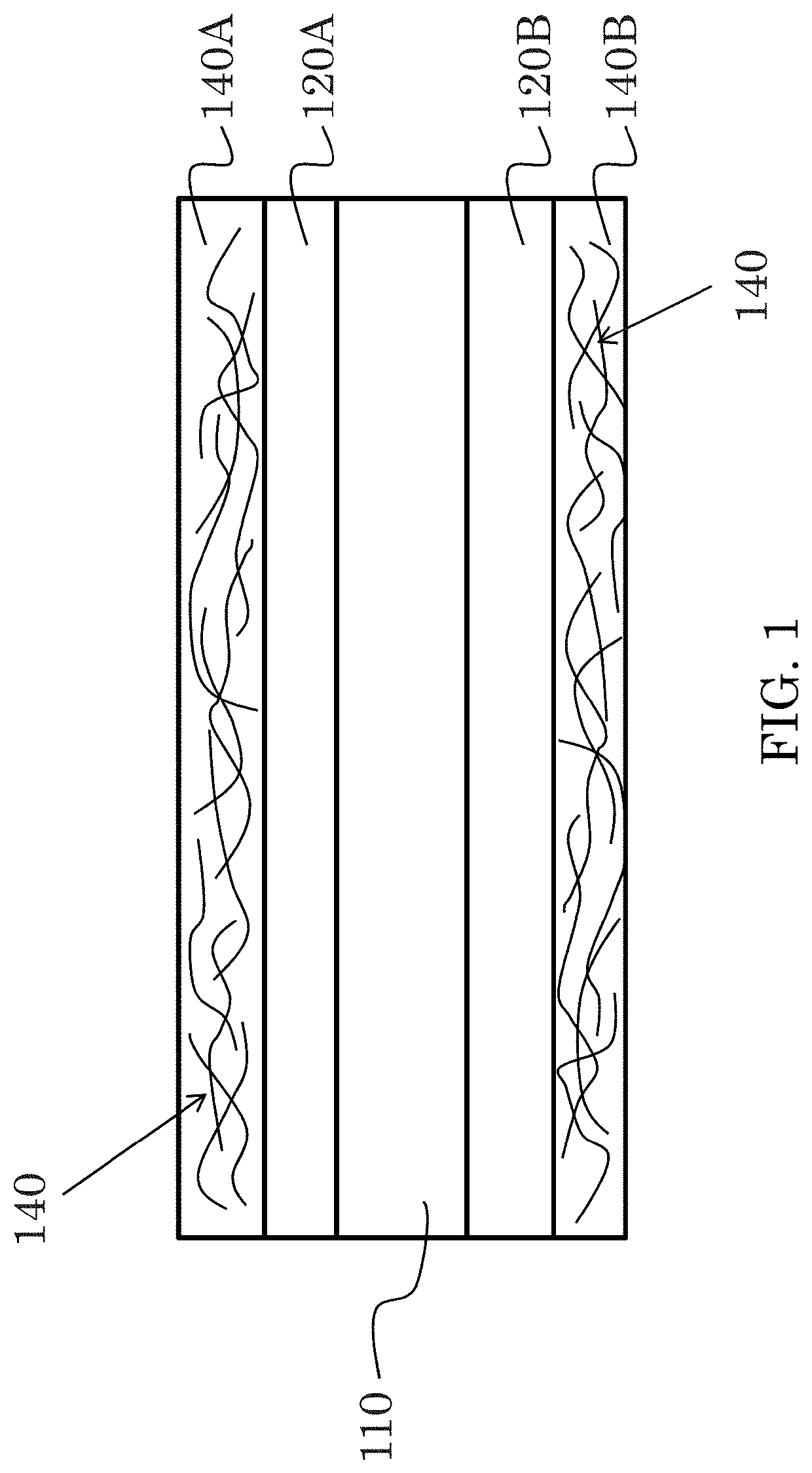
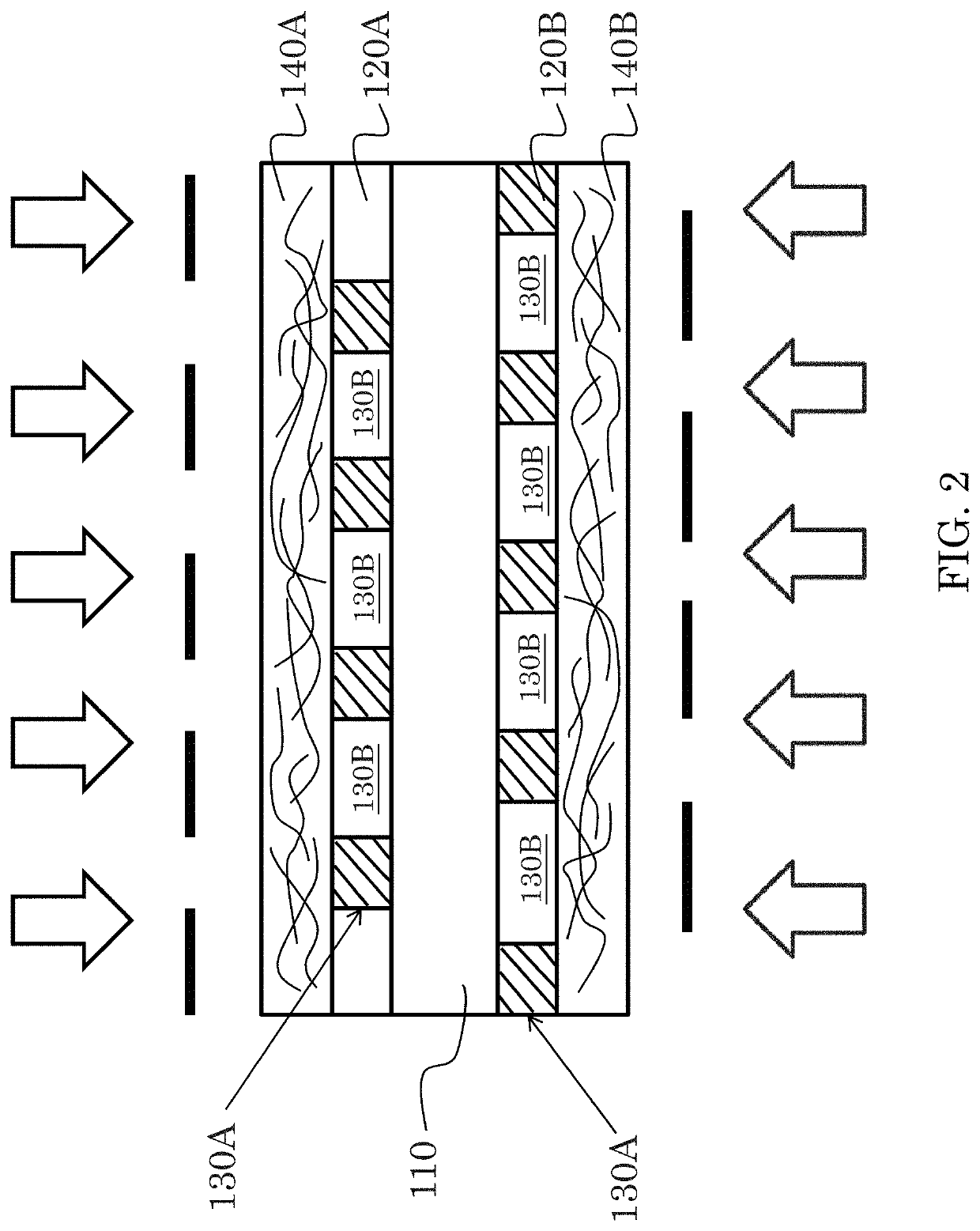
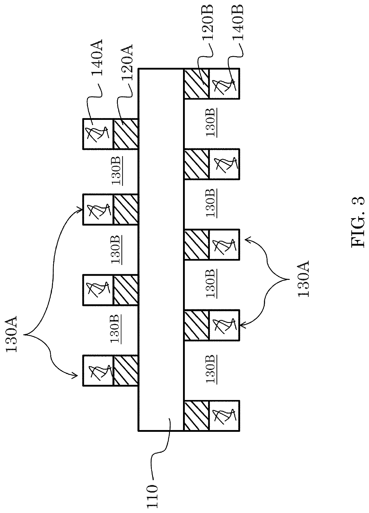
[0040]FIGS. 1 to 3 are schematic diagrams showing the steps of the manufacturing method of a double-sided electrode structure according to some embodiments of this disclosure. Th...


PUM


Abstract

A patterning process for forming a double-sided electrode structure includes: providing a substrate having two opposite surfaces, wherein a first photo-sensitive layer and a second photo-sensitive layer are respectively formed on the opposite surfaces; forming a first metal nanowire layer on the first photo-sensitive layer and a second metal nanowire layer on the second photo-sensitive layer; and performing a double-sided lithography process. The lithography process includes: performing an exposure process to define a removing area and a remaining area on both of the first and the second photo-sensitive layers; and removing the first and second photo-sensitive layers and the first and second metal nanowire layers in the defined removing areas by a developer solution, thereby patterning the first and second metal nanowire layers.

Description

CROSS REFERENCE TO RELATED APPLICATIONS[0001]This Non-provisional application claims priority under 35 U.S.C. § 119(a) to Patent Application No. 201810541243.4 filed in People's Republic of China on May 30, 2018, the entire contents of which are hereby incorporated by reference.BACKGROUNDTechnology Field[0002]The present disclosure relates to a double-sided electrode structure and a patterning process thereof.Description of Related Art[0003]Transparent conductive material, which has good light transmission and electrical conductivity, is generally applied in various display devices or touch devices. In many applications, the transparent conductive material is a metal oxide, such as indium tin oxide (ITO), indium zinc oxide (IZO), cadmium tin oxide (CTO), or aluminum-doped zinc oxide (AZO). A thin film of the metal oxide is formed by physical vapor deposition (PVD) or chemical vapor deposition (CVD), and then patterned by a laser process to form, for example, a touch sensor. However,...

Claims


Application Information

Patent Timeline
IPC IPC(8): H01L27/12G06F3/041H05K3/06H05K1/09
CPCH01L27/1262G06F3/0412H05K3/06H05K2201/0326H01L27/124H05K1/09G06F2203/04103H01L27/1259G06F2203/04112G06F3/0445
Inventor HSIAO, CHUNG-CHINLIEN, SIOU-CHENGTSAI, CHIA-YANG
Owner CAMBRIOS FILM SOLUTIONS CORP
Why Eureka
Try Eureka