Multi-wafer stack structure and forming method thereof

a stack structure and multi-wafer technology, applied in the direction of electrical equipment, semiconductor devices, semiconductor/solid-state device details, etc., can solve the problems of reducing signal transmission speed, high cost, and large overall so as to meet the requirements of thinning and thinning of semiconductor products, reduce the overall device thickness of multi-wafer stack packages, and increase the density of packages

Active Publication Date: 2020-03-05
WUHAN XINXIN SEMICON MFG CO LTD
View PDF0 Cites 1 Cited by
  • Summary
  • Abstract
  • Description
  • Claims
  • Application Information

AI Technical Summary

Benefits of technology

[0005]An objective of the present invention is to provide a multi-wafer stack structure to reduce the overall thickness of multi-wafer stacking.
[0006]Another objective of the present invention is to increase the signal transmission speed and reduce the power loss without using wires.
[0026]In the multi-wafer stack structure and method provided by the present invention, the first interconnection layer is electrically connected to the second metal layer and the first metal layer via the first opening, the second interconnection layer is electrically connected to the first interconnection layer via the second opening, the third interconnection layer is electrically connected to the third metal layer via the third opening, and the second interconnection layer is in contact with the third interconnection layer, so that there is no need to reserve the wire pressure welding space between the wafers and the silicon substrate is eliminated, thereby achieving multi-wafer interconnection and reducing the thickness of the multi-wafer stacking. Therefore, the overall device thickness of the multi-wafer stack package is reduced, the package density is increased, and the requirements for semiconductor products to become thinner and thinner are met. Moreover, the multi-wafer stack structure no longer needs a wire, and the design processing of the silicon substrate and the plurality of common pads on the silicon substrate is eliminated, which is advantageous in reducing the cost and simplifying the process. In addition, the second interconnection layer is in contact with the third interconnection layer to shorten the interconnection distance between wafers, thereby reducing the parasitic capacitance and power loss, and increasing the transmission speed.

Problems solved by technology

However, the inventors have found that there are some problems with the traditional multi-wafer wire interconnection method.
First, there are restrictions on the development of multi-wafer stacking to high-density thickness, the wire pressure welding space needs to be reserved between the multiple wire-bonded wafers, the silicon substrate itself also has a certain thickness, and the overall thickness is large after the multiple wafers are stacked to some extent.
Besides, the wire is usually a gold wire which is high in cost, the wire leads to a relatively long interconnection line, and the long interconnection line reduces the signal transmission speed and increases the power loss.
In addition, the silicon substrate cannot meet the need of multi-wafer stacking high-density development for more and more common pads.

Method used


Image

  • Multi-wafer stack structure and forming method thereof
  • Multi-wafer stack structure and forming method thereof
  • Multi-wafer stack structure and forming method thereof

Examples


Embodiment Construction

[0050]Hereinafter, a multi-wafer stack structure and method according to the present invention will be further described in detail with reference to the accompanying drawings and specific embodiments. Advantages and features of the present invention will become more apparent from the following description. It should be noted that the drawings are in a very simplified form and are used in a non-precise scale, and are merely for convenience and clarity of the purpose of the embodiments of the present invention.

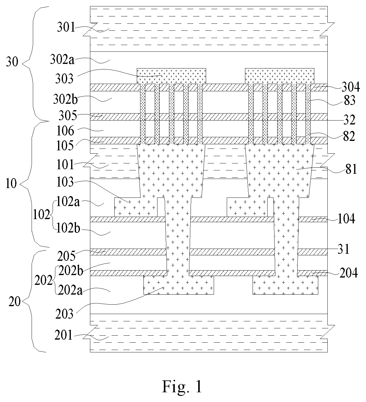
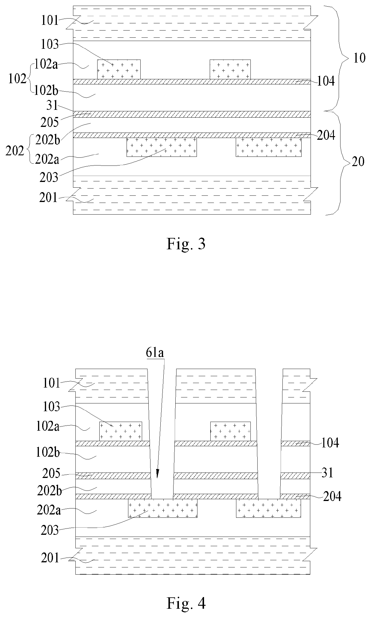
[0051]The multi-wafer stack structure provided by the embodiment of the present invention is described in detail below with reference to FIG. 1, FIG. 6, FIG. 9 and FIG. 10. A multi-wafer stack structure includes:

[0052]a first wafer 10, where the first wafer 10 includes a first substrate 101, a first dielectric layer 102 located on the first substrate 101 and a first metal layer 103 embedded in the first dielectric layer 102;

[0053]a second wafer 20, where the second wafer 20 incl...


PUM

PropertyMeasurementUnit
dielectricaaaaaaaaaa
density thicknessaaaaaaaaaa
thicknessaaaaaaaaaa

Abstract

A multi-wafer stack structure and fabricating method thereof are disclosed. In the multi-wafer stack structure, the first interconnection layer is electrically connected to the second metal layer and the first metal layer via the first opening, the second interconnection layer is electrically connected to the first interconnection layer via the second openings, the third interconnection layer is electrically connected to the third metal layer via the third openings, and the second interconnection layer is in contact with the third interconnection layer, so that there is no need to reserve the wire pressure welding space between the wafers and a silicon substrate is eliminated, the overall device thickness of the multi-wafer stack package is reduced. Moreover, the design processing of the silicon substrate and a plurality of common pads on the silicon substrate is eliminated, thereby reducing the parasitic capacitance and power loss, and increasing the transmission speed.

Description

CROSS-REFERENCE TO RELATED APPLICATION[0001]This application claims the priority of Chinese patent application number 201810988464.6, filed on Aug. 28, 2018, the entire contents of which are incorporated herein by reference.TECHNICAL FIELD[0002]The present invention pertains to the technical field of integrated circuit manufacturing, and in particular, relates to a multi-wafer stack structure and a forming method thereof.BACKGROUND[0003]In the trend of highly integrated semiconductor development, wire bonding is often used after multi-wafer stacking to achieve interconnections between multiple wafers. Specifically, multiple wafers are stacked vertically on a dedicated silicon substrate, each wafer has a plurality of pads for interconnection, the silicon substrate has a plurality of common pads, one end of the wire is pressure-bonded to the pad of the wafer, and the other end of the wire is collectively pressure-bonded to the common pad of the silicon substrate, thereby achieving int...

Claims


Application Information

Patent Timeline
Patent Type & Authority Applications(United States)
IPC IPC(8): H01L25/065H01L23/522H01L23/31H01L21/768
CPCH01L23/5226H01L21/76805H01L25/0657H01L23/3171H01L21/76832H01L23/3192H01L21/76802H01L21/76877H01L23/5283H01L21/76898H01L23/481H01L25/50H01L2225/06544
Inventor ZHAO, CHANGLINLIU, TIANJIAN
Owner WUHAN XINXIN SEMICON MFG CO LTD
Why Eureka
Try Eureka