Inspection device

a technology of charge particle and inspection device, which is applied in the direction of basic electric elements, electric discharge tubes, electrical apparatus, etc., can solve the problems of difficult above, and achieve the effects of reducing the number of imaging times, high throughput in inspection, and reducing the time taken for auto-focusing

Active Publication Date: 2020-11-19
HITACHI LTD
View PDF0 Cites 0 Cited by
  • Summary
  • Abstract
  • Description
  • Claims
  • Application Information

AI Technical Summary

Benefits of technology

[0013]To recap the above, in order to shorten the inspection time by an electron microscope, to shorten the time taken for auto-focusing is effective. Therefore, it is enabled to estimate the defocus amount (relative shift amount from the best focus position) or at least the direction of defocusing (the sign of (z_best-z_0)) hopefully from one sheet or an extremely small number of sheets of the image. The estimation should be such one that is not affected by blurring of the contour caused by the shape of the object pattern. Also, in order to achieve the accuracy of a same as or higher than the degree of the prior art, a procedure of assuring reliability of estimation and further improving the accuracy is required.
[0015]The inspection device that is another embodiment of the present invention is an inspection device that observes patterns formed on a sample at plural inspection spots, the inspection device including a charged particle optical system that includes a charged particle beam source emitting a charged particle beam and plural lenses focusing the charged particle beam on the sample, a detector that detects secondary charged particles emitted by an interaction of the charged particle beam and the sample, and a calculation unit that executes auto-focusing at a time a field of view of the charged particle optical system moves over the plural inspection spots, in which, in executing the auto-focusing, the calculation unit irradiates the charged particle beam to the sample under an optical condition that is for observing the pattern by the charged particle optical system, acquires a first image and a second image, the first image being formed from a signal outputted by the detector in detecting the secondary charged particles, a focus point of the charged particle beam being shifted from that of the time when the first image is acquired in the second image, the first image and the second image including a line pattern image or a space pattern image extending in one direction, and determines a direction for eliminating a position shift between a focus position of the charged particle beam of the time when the first image is acquired and a best focus position based on a magnitude relation between a width of the line pattern image or the space pattern image in the first image and a width of the line pattern image or the space pattern image in the second image, and a shift amount between a focus position of the charged particle beam of the time when the first image is acquired and a focus position of the charged particle beam of the time when the second image is acquired is made within a depth of focus of the inspection device.
[0016]According to the present invention, by reducing the number of times of imaging for estimating the best focus position, the time taken for auto-focusing can be reduced. As a result, it is allowed to provide a charged particle beam device having a high throughput in inspection of a pattern forming step and an inspection device using the same.

Problems solved by technology

However, the above is not easy.

Method used


Image

  • Inspection device
  • Inspection device
  • Inspection device

Examples


first embodiment

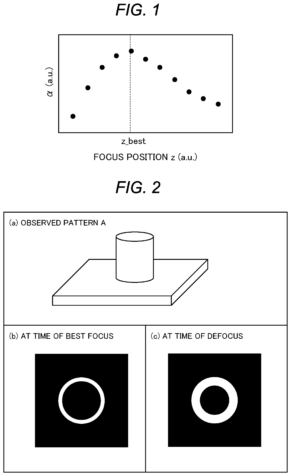
[0088]According to a first embodiment, the inspection time is shortened by determining the focusing condition of the image for inspection and executing inspection according to the defocus amount estimated from one sheet of the image. Also, the effect shown here is obtained by simulation.

[0089]According to the method used in the first embodiment, in the table of FIG. 13, the calculation method is the artificial intelligence, the learning / determining pictorial figure is a same pictorial figure, the object datum is the image, and the operation method is combination of “determination within depth of focus+movement to best focus”. The CNN is used in estimating the defocus amount from the image.

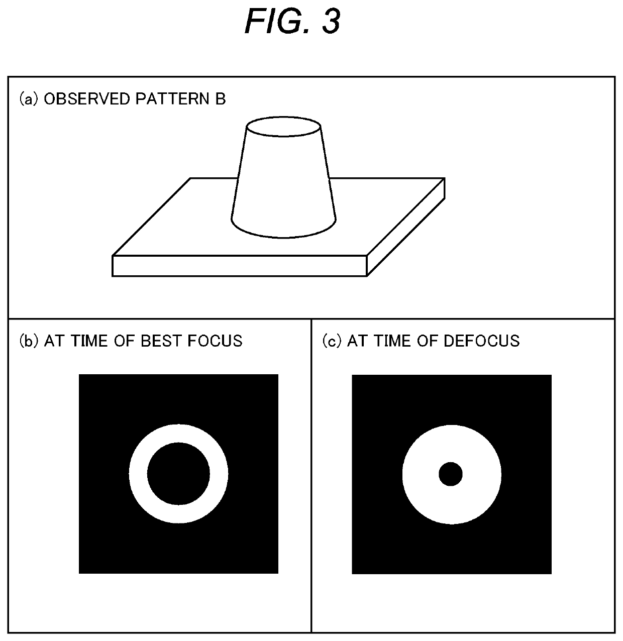
[0090]First, explanation will be given with respect to a procedure for constructing a CNN that executes defocusing estimation by learning. The user observed a hole pattern 40 nm in diameter formed in a silicon wafer using a SEM, and acquired an image. At the time of imaging, after eliminating vario...

second embodiment

[0095]According to a second embodiment, the inspection time is shortened by executing the inspection determining the focusing condition of the image for inspection according to the defocus amount estimated from one sheet of the image. The effect shown here is also secured by simulation.

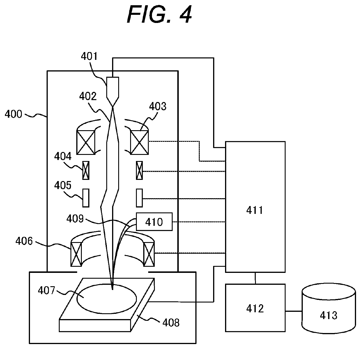
[0096]According to the method used in the second embodiment, in the table of FIG. 13, the calculation method is the index, the object datum is the contour, and the operation method is combination of “determination within depth of focus+movement to best focus+execution of conventional AF”. According to the second embodiment, a contour line becoming a closed curve is extracted from the same dot pattern image as that of the first embodiment, the focus position is corrected based on a defocus amount estimated by indexing the shape of the contour line, and the inspection is executed. The inspection object is a dot pattern with 40 nm of the diameter formed in the silicon wafer. With respect to the image hav...

third embodiment

[0100]According to a third embodiment, the inspection time is shortened by executing the inspection determining the focusing condition of the image for inspection according to the defocus amount estimated from one sheet of the image.

[0101]According to the method used in the third embodiment, in the table of FIG. 13, the calculation method is the artificial intelligence, the learning / determining pictorial figure is a different pictorial figure, splitting is executed for the learning data (the method B), the object datum is the contour, and the operation method is combination of “determination within depth of focus+movement to best focus+execution of conventional AF”. The CNN is used in estimating the defocus amount from the image.

[0102]First, explanation will be given with respect to a procedure for constructing a CNN that executes defocusing estimation by learning. With respect to the same silicon wafer as that of the first embodiment, 5,100 sheets of the images are obtained in tota...


PUM


Abstract

An inspection device includes a charged particle optical system that includes a charged particle beam source emitting a charged particle beam and plural lenses focusing the charged particle beam on a sample, a detector that detects secondary charged particles emitted by an interaction of the charged particle beam and the sample, and a calculation unit that executes auto-focusing at a time a field of view of the charged particle optical system moves over plural inspection spots, the calculation unit irradiates the charged particle beam to the sample under an optical condition that is obtained by introducing astigmatism of a predetermined specification to an optical condition that is for observing a pattern by the charged particle optical system, and executes the auto-focusing using an image formed from a signal outputted by the detector in detecting the secondary charged particles.

Description

CROSS-REFERENCE TO RELATED APPLICATION[0001]This application claims priority to Japanese Patent Application No. 2019-093640 filed on May 17, 2019, the entire contents of which are incorporated by reference herein.BACKGROUND OF THE INVENTION[0002]The present invention relates to an inspection device using a charged particle beam image.BACKGROUND ART[0003]In the manufacturing process of a semiconductor device, there has occurred necessity of shortening also the time taken for inspection and dimension measurement (will be hereinafter collectively referred to as an inspection) in order to reduce the total cost. Therefore, improvement of throughput has been required with respect also to a Scanning Electron Microscope (SEM) that observes a fine pattern in the middle of the manufacturing step.[0004]Although the fine pattern is imaged with high resolution in an inspection step by a SEM, in order to achieve high resolution, there is required a function of automatically focusing the object pa...

Claims


Application Information

Patent Timeline
Patent Type & Authority Applications(United States)
IPC IPC(8): H01J37/22H01J37/28H01J37/244H01J37/10H01J37/30H01J37/21
CPCH01J2237/30427H01J37/3005H01J2237/216H01J37/244H01J2237/1532H01J2237/2817H01J37/28H01J37/10H01J37/21H01J37/222H01J2237/2448H01J37/265
Inventor SHINTANI, ATSUKOSOHDA, YASUNARITAKAHASHI, NORITSUGUKOYAMA, HIKARU
Owner HITACHI LTD
Why Eureka
Try Eureka