Chip-scale optical interconnect using microleds

an optical interconnect and micro-led technology, applied in the direction of electrical equipment, semiconductor devices, instruments, etc., can solve the problems of consuming a large amount of electrical power, consuming a large amount of power, and consuming electrical power, and achieve the effect of low power and low cos

Active Publication Date: 2020-12-31
AVICENATECH CORP
View PDF0 Cites 7 Cited by
  • Summary
  • Abstract
  • Description
  • Claims
  • Application Information

AI Technical Summary

Benefits of technology

[0014]Aspects of some embodiments utilize advances in unrelated fields of optical devices for displays and waveguide structures for control of three-dimensional (3D) beams together, breaking the technological barriers in short distance data communications and providing for implementation of devices that can form data connections that are potentially fast, low power, and low cost, at short distances. This can help synchronize the clock signal on a chip, transfer data across a chip, connect ICs with memory, and connect to other peripherals.

Problems solved by technology

However, at lengths below a meter, interconnects remain electrical and are barriers for performance.
Integrated circuits such as CPUs and GPUs are large, and sending data and clock signals across the silicon chip may be limited by the RC time constants of the interconnect metal.
Getting information off the chip to co-packaged memory and connecting to peripherals all consume a great deal of power as electrical interconnects are lossy, distort the signal, and have capacitance that takes electrical power to charge up.
Clock and data recovery circuits often must be used to periodically clean up the signal, which takes considerable electrical power.
In addition to the RC and loss issues of electrical wiring, there is there also the limit that these interconnects are often confined to a 2D plane for example, on the surface of chips, ceramic packages, silicon interposers, or circuit boards.
The electrical interconnect issue at short distance scales has become a critical barrier as Moore's Law has slowed.
The increased importance of artificial intelligence circuits and graphical processing units are all limited by this communication barrier at shorter distances.
Difficulty with clock synchronization on chip, limited memory bandwidth, and long latency to access data, are all choking high speed computation.
The amount of memory available and the latency in accessing data from memory is a serious limitation brought on by the limits of electrical interconnects.
But there is a limit to how much cache can be integrated.
But this is of course at the price of higher latency and slower transfer rate.
On the transmission side, lasers are generally unsuitable for use in large numbers for short distance interconnects.
They are typically grown on III-V materials that are incompatible with silicon, with yields that are far below electronic devices in silicon.
Lasers also have threshold currents of about a few milliamps, which wastes power.
Using an external laser and on-chip modulators has been investigated, but waveguide modulators are lossy, consume a great deal of electrical power and are typically the same size as edge-emitting lasers.
Vertical cavity modulators are temperature sensitive and difficult to use.
However, silicon photonics is also lossy and consumes the same amount of power as III-V components.
The medium is also an issue.
Coupling optical fibers to silicon chips and the integration of lateral optical waveguides with copackaged lasers and electronics is complicated and expensive.

Method used


Image

  • Chip-scale optical interconnect using microleds
  • Chip-scale optical interconnect using microleds
  • Chip-scale optical interconnect using microleds

Examples


Embodiment Construction

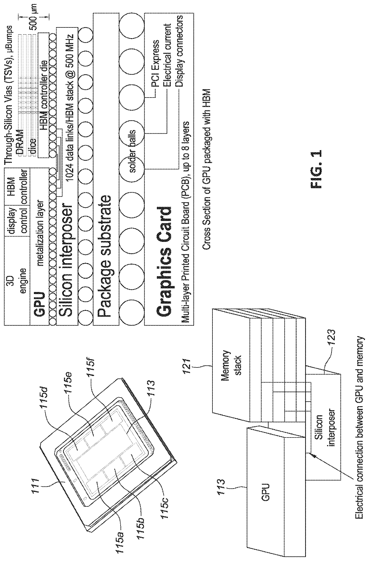
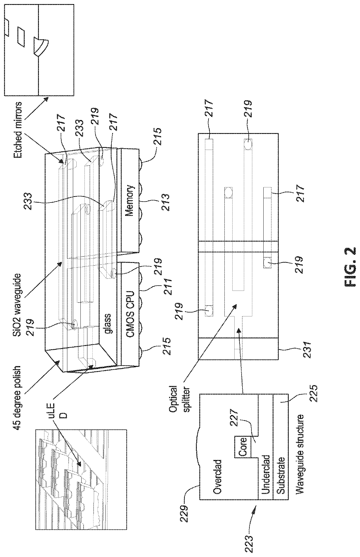
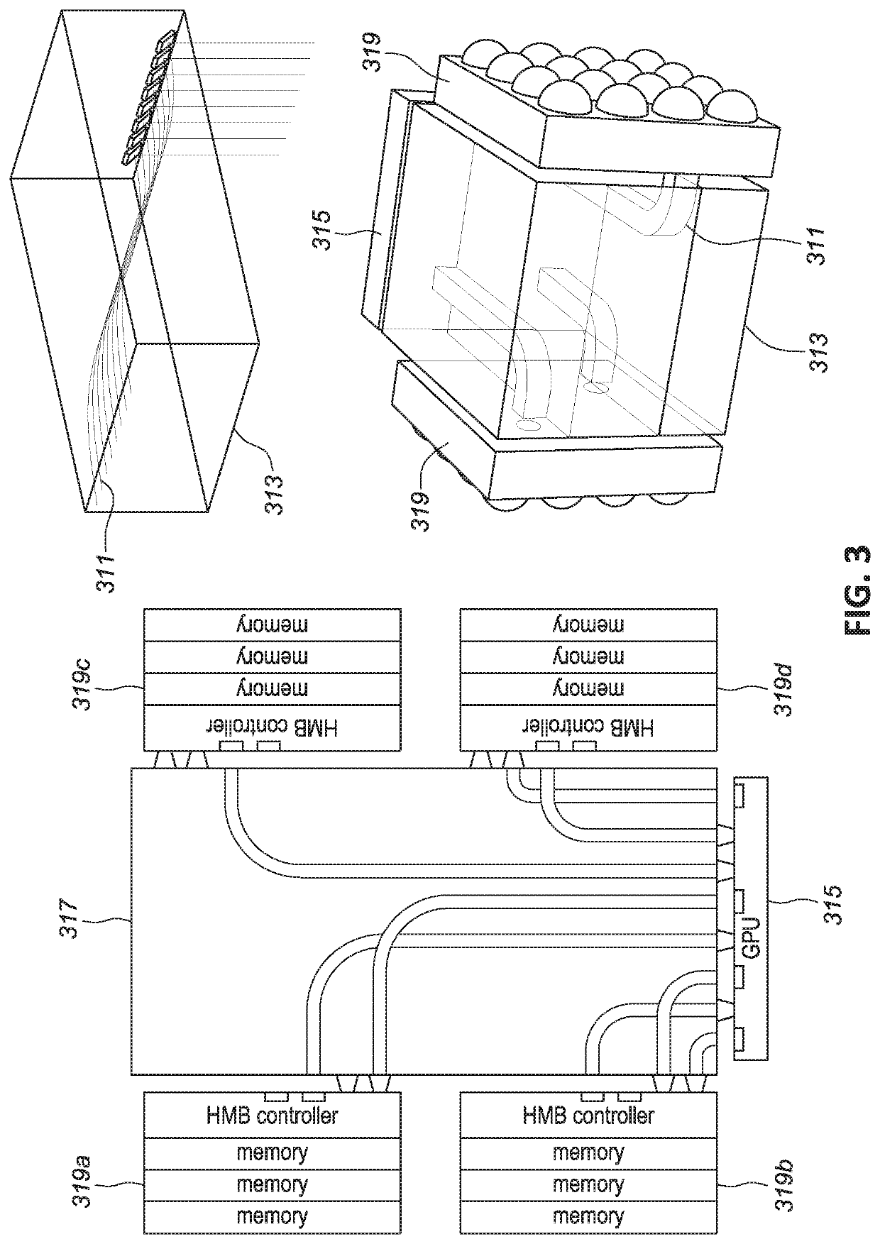
[0034]Embodiments in accordance with this invention use LEDs, microLEDs in various embodiments, for inter-chip communication, with in some embodiments the chips in communication being within a common package or on a common package substrate. Some embodiments use an array of microLEDs, such as blue LEDs on the order of 2 um×2 um each. In some embodiments a microLED is distinguished from a semiconductor laser (SL) as follows: (1) a microLED does not have an optical resonator structure; (2) the optical output from a microLED is almost completely spontaneous emission, whereas the output from a SL is dominantly stimulated emission; (3) the optical output from a microLED is temporally and spatially incoherent, whereas the output from a SL has significant temporal and spatial coherence; (4) a microLED is designed to be driven down to a zero minimum current, whereas a SL is designed to be driven down to a minimum threshold current, which is typically at least 1 mA. In some embodiments a mic...


PUM

PropertyMeasurementUnit
lengthaaaaaaaaaa
threshold currentaaaaaaaaaa
sizesaaaaaaaaaa

Abstract

In package intra-chip and/or inter-chip optical communications are provided using microLEDs and photodetectors mounted to integrated circuit (IC) chips and/or to transceiver dies associated with the IC chips. Light from the LEDs may pass through waveguides on or in a substrate to which the IC chips are mounted or which couple the IC chips.

Description

CROSS REFERENCE TO RELATED APPLICATION[0001]This application claims the benefit of the filing date of U.S. Provisional Patent Application No. 62 / 867,448, filed on Jun. 27, 2019, and U.S. Provisional Patent Application No. 62 / 900,383, filed on Sep. 13, 2019, the disclosures of which are incorporated by reference herein.BACKGROUND OF THE INVENTION[0002]The present application relates generally to high speed electronic packaging with short-distance connections use optical links.[0003]Optical interconnects have replaced electrical connections over time. The low optical loss of the optical fiber, the intrinsically high bandwidth of light, the lack of interference, and the absence of parasitic inductance and capacitance, are all characteristics that favor the modulation of light for interconnects. Starting at long lengths, the advantages of optics has proven itself over shorter distance scales over time. Today, the highest speed links over a few meters are almost always optical. In the la...

Claims


Application Information

Patent Timeline
Patent Type & Authority Applications(United States)
IPC IPC(8): H01L27/15G02B6/43G02B6/42
CPCG02B6/43G02B6/4257G02B6/4214H01L27/156H01L25/167G02B6/4286G02B6/4298H01L25/0753G02B6/12002H01L2224/16225H01L31/0203
Inventor PEZESHKI, BARDIAKALMAN, ROBERT
Owner AVICENATECH CORP
Why Eureka
Try Eureka