Semiconductor device, method of fabricating same and memory

a semiconductor and memory technology, applied in the field of semiconductor technology, can solve the problems of slowing down the fabrication process, reducing the productivity and utilization rate of fabrication equipment, and affecting the production efficiency of semiconductor fabrication equipment, so as to accelerate the fabrication and increase the throughput

Active Publication Date: 2021-03-18
FUJIAN JINHUA INTEGRATED CIRCUIT CO LTD
View PDF0 Cites 3 Cited by
  • Summary
  • Abstract
  • Description
  • Claims
  • Application Information

AI Technical Summary

Benefits of technology

[0005]It is an objective of the present invention to provide a semiconductor device which can be fabricated in an easier way, thus expediting the fabrication and resulting in a higher throughput.
[0018]In the semiconductor device provided in the present invention, each bit line contact plug partially resides on the insulating material layer and is coupled to the active area. That is to say, in addition to the active area, the bit line contact plug additionally extends laterally over part of the buried gate. Such an increased width of the bit line contact plug can maximize its contact area, and thus minimize its contact resistance, with the active area. As a result, even when there is a void within the bit line contact plug, its sufficient contact with the active area can still ensure good signal transmission therewith. Additionally, such a bit line contact plug allowed to contain a void can be fabricated using a rapid deposition process, which can expedite the fabrication of the bit line contact plug itself and hence of the semiconductor device. This can result in an enhanced throughput and higher utilization of the semiconductor fabrication equipment.

Problems solved by technology

The ever-advancing semiconductor technology is leading to increasing miniaturization of semiconductor devices, which in turn makes the fabrication of such devices more difficult, less productive and less efficient in the utilization of semiconductor fabrication equipment.
This would slow down the fabrication and lower both the productivity and utilization rate of fabrication equipment.

Method used


Image

  • Semiconductor device, method of fabricating same and memory
  • Semiconductor device, method of fabricating same and memory
  • Semiconductor device, method of fabricating same and memory

Examples


embodiment 1

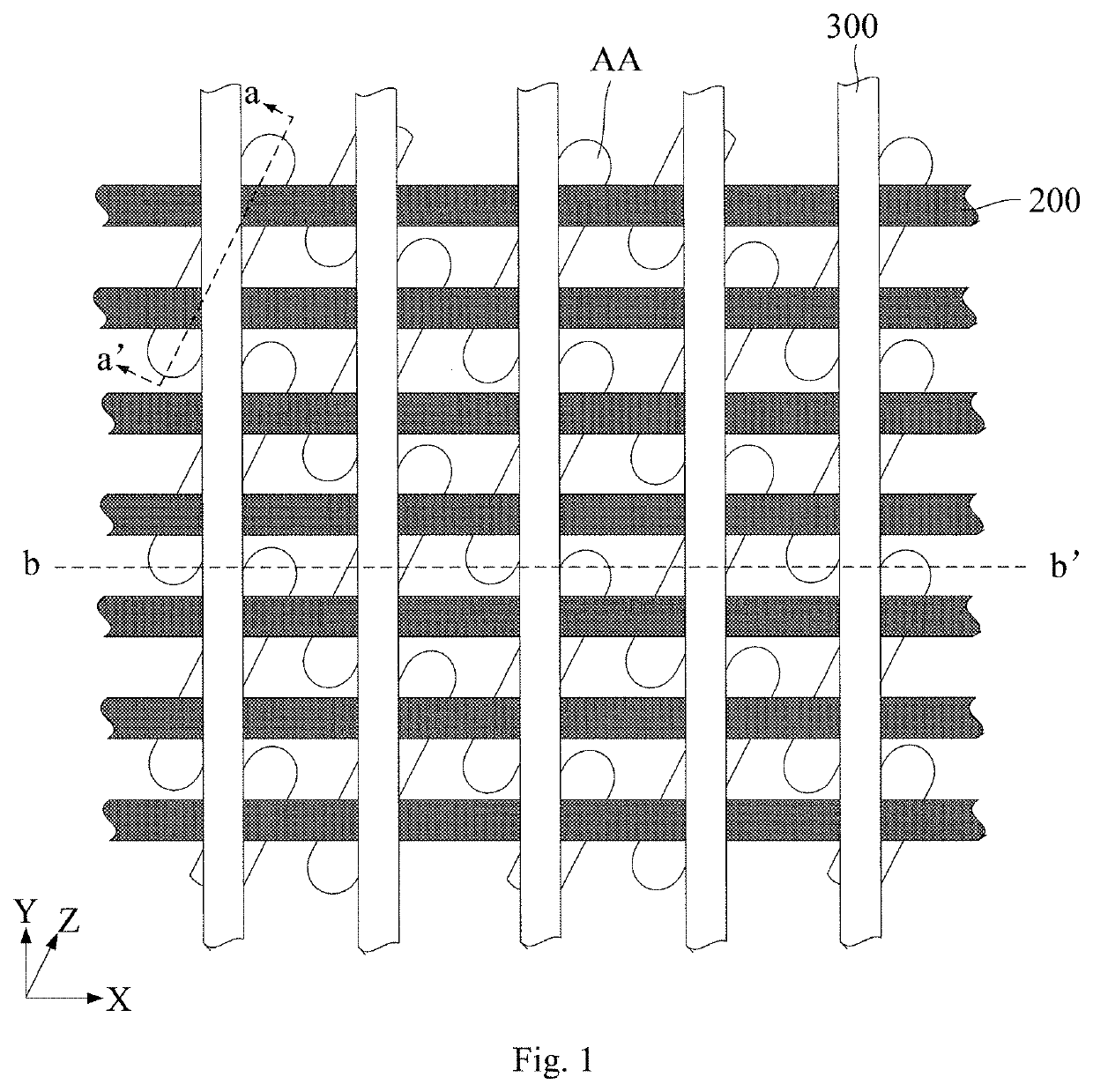
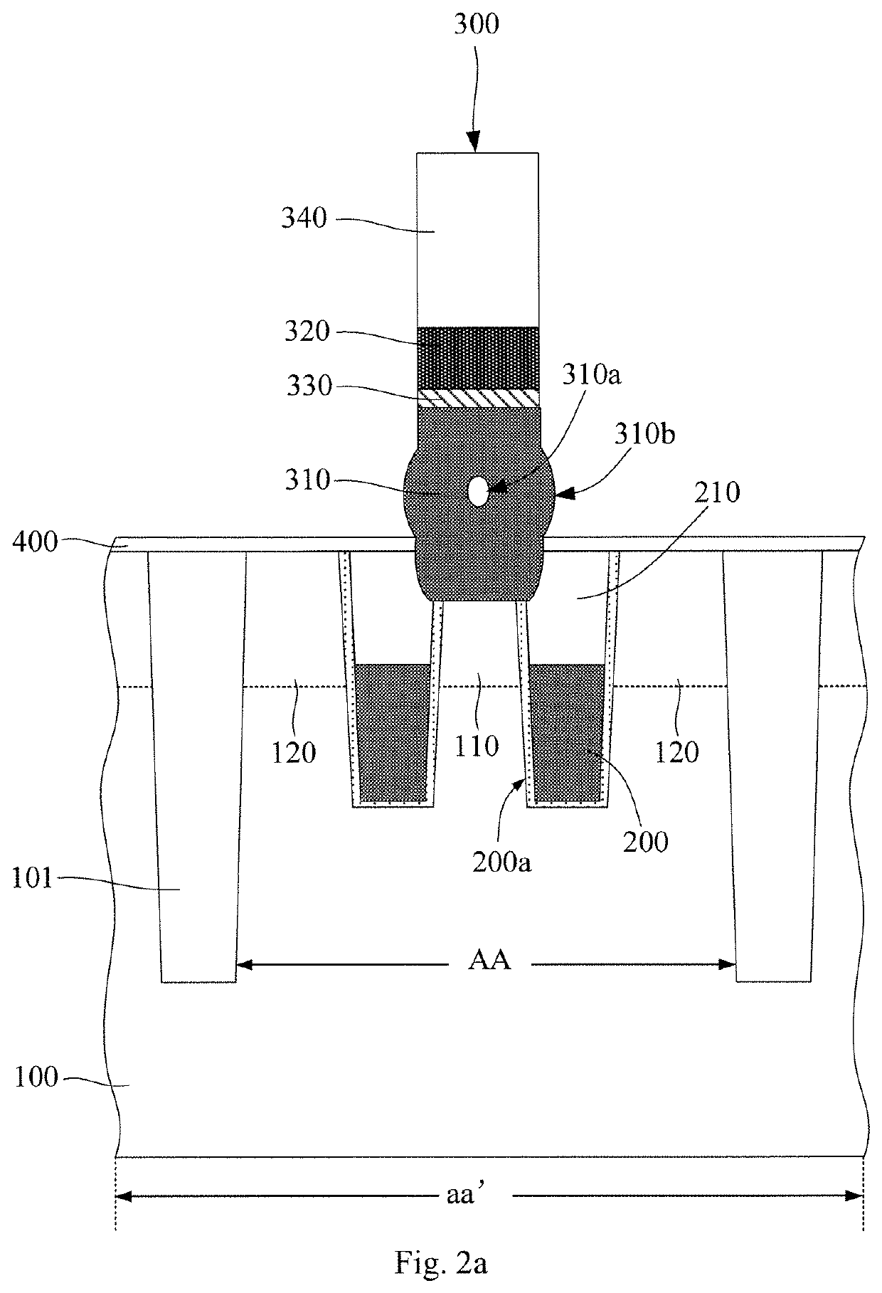
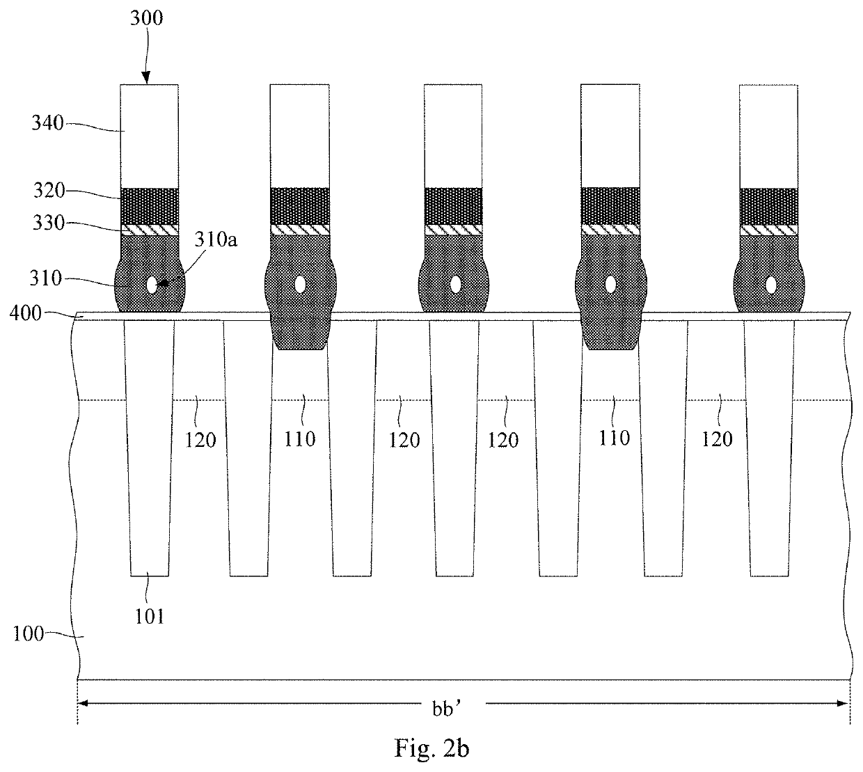
[0048]FIG. 1 is a top view of a semiconductor device according to a first embodiment of the present invention. FIG. 2a is a cross-sectional view of the semiconductor device of FIG. 1 taken along line aa′, while FIG. 2b is a cross-sectional view of the semiconductor device of FIG. 1 taken along line bb′.

[0049]As shown in FIGS. 1 and 2a-2b, the semiconductor device includes a substrate 100 as well as buried gates 200 and bit lines 300 formed in / on the substrate 100.

[0050]Further, the substrate 100 is formed therein with a plurality of active areas AA. The semiconductor device may be implemented as, for example, a memory. This embodiment will be explained below with the semiconductor device being a memory as an example. To this end, in each of the active areas AA, first source / drain regions 110 and second source / drain regions 120 may be formed to constitute storage transistors. Adjacent active areas AA may be isolated from each other by, for example, trench isolation structures 101.

[00...

embodiment 2

[0116]This embodiment differs from Embodiment 1 in a trapezoidal cross-section of the bit line contact plug, which has a top base and a bottom base longer than the top base. That is, the bit line contact plug according to this embodiment gradually widens from the top downward so as to ensure sufficient contact at the bottom with the active area.

[0117]FIG. 5 is a schematic diagram showing the structure of a semiconductor device according to this Embodiment 2. As shown in FIG. 5, the bit line contact plug 310′ has a trapezoidal cross-section in the direction perpendicular to the first direction (i.e., the bit line contact plug 310′ has a trapezoidal cross-section in the width-wise direction). The bit line contact plug 310′ has a lower portion extending from the upper surface of the insulating material layer 210 to the predetermined depth. The lower portion also has a trapezoidal cross-section with a top base and a bottom base longer than the top base.

[0118]In this embodiment, the bott...


PUM

PropertyMeasurementUnit
depthaaaaaaaaaa
widthaaaaaaaaaa
conductiveaaaaaaaaaa

Abstract

A semiconductor device, a method of fabricating the semiconductor device and a memory are disclosed. In the provided semiconductor device, bit line contact plugs partially reside on insulating material layers in gate trenches in active areas and thus can come into sufficient contact with the active areas. This ensures good electrical transmission between the bit line contact plugs and the active areas even when there are internal voids in the bit line contact plugs. Such bit line contact plugs allowed to contain internal voids can be fabricated in an easier and faster manner, thus allowing a significantly enhanced memory fabrication throughput.

Description

TECHNICAL FIELD[0001]The present invention relates to the field of semiconductor technology and, in particular, to a semiconductor device, a method of fabricating the semiconductor device and a memory.BACKGROUND[0002]The ever-advancing semiconductor technology is leading to increasing miniaturization of semiconductor devices, which in turn makes the fabrication of such devices more difficult, less productive and less efficient in the utilization of semiconductor fabrication equipment.[0003]For example, a memory, such as a dynamic random access memory (DRAM), typically includes storage transistors, as well as bit lines and word lines for selection of a corresponding storage transistor by using the bit lines and the word lines and activation of the selected storage transistor.[0004]During the fabrication of an existing memory, in order to ensure good electrical connections between bit lines and storage transistors, the processes used to form the bit lines (in particular, contact plugs...

Claims


Application Information

Patent Timeline
Patent Type & Authority Applications(United States)
IPC IPC(8): H01L27/108
CPCH01L27/10888H01L27/10876H01L27/10823H01L27/10814H10B12/312H10B12/01H10B12/00H10B12/34H10B12/482H10B12/485H10B12/053H10B12/315
Inventor HE, SHI-WEIHUANG, TE-HAOCHU, HSIEN-SHIHCHOU, YUN-FANHUANG, FENG-MING
Owner FUJIAN JINHUA INTEGRATED CIRCUIT CO LTD
Why Eureka
Try Eureka