Thinned semiconductor chip with edge support

Active Publication Date: 2021-09-16
DIODES INC
View PDF11 Cites 0 Cited by
  • Summary
  • Abstract
  • Description
  • Claims
  • Application Information

AI Technical Summary

Benefits of technology

This patent discusses a new design for computer chips that reduces device resistance and power dissipation. The design includes a thicker chip at the edges, which improves mechanical strength, and a thin and flat chip near the circuit elements. This reduces the impact of the chip's periphery on its overall performance. The design also utilizes a back side metal layer to provide a favorable current path for reducing device resistance and power dissipation. Overall, this design optimizes chip performance and efficiency.

Problems solved by technology

One possible reason is that the models fail to adequately consider the detrimental effect of the complex and uneven chip topography thus created on the current flow.
The turbulence in current flow results in higher local current density and higher ohmic heat, and higher power loss.
And, in high frequency switching applications, adding metal layer with thickness beyond the skin depth of the signals does not contribute appreciably to total resistance reduction.

Method used


Image

  • Thinned semiconductor chip with edge support
  • Thinned semiconductor chip with edge support
  • Thinned semiconductor chip with edge support

Examples


Embodiment Construction

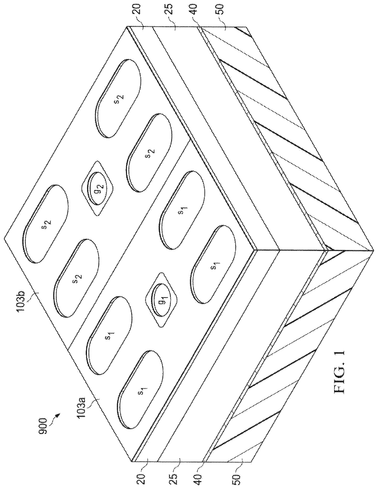
[0034]FIG. 1 depicts a perspective view of a semiconductor device 900 that embodies certain aspects of this invention. In this embodiment, elements 20 and 25 are silicon, in which element 25 is a substrate layer, element 20 is an epitaxial layer grown on top of the substrate layer 25. The electrical resistivity of the epitaxial layer 20 is higher than the resistivity of the substrate 25. Layer 20 and layer 25 Layer combine to make up the semiconductor chip in the device 900. Layer 40 is a metal layer and is referred to as the back-side metal layer, which makes ohmic contact to the back side of the silicon chip. Layer 50 is a non-conductive layer, which in this embodiment comprises a molding compound, an epoxy material mixed with filler particles. Layer 50 has a flat and smooth back side suitable for laser marking.

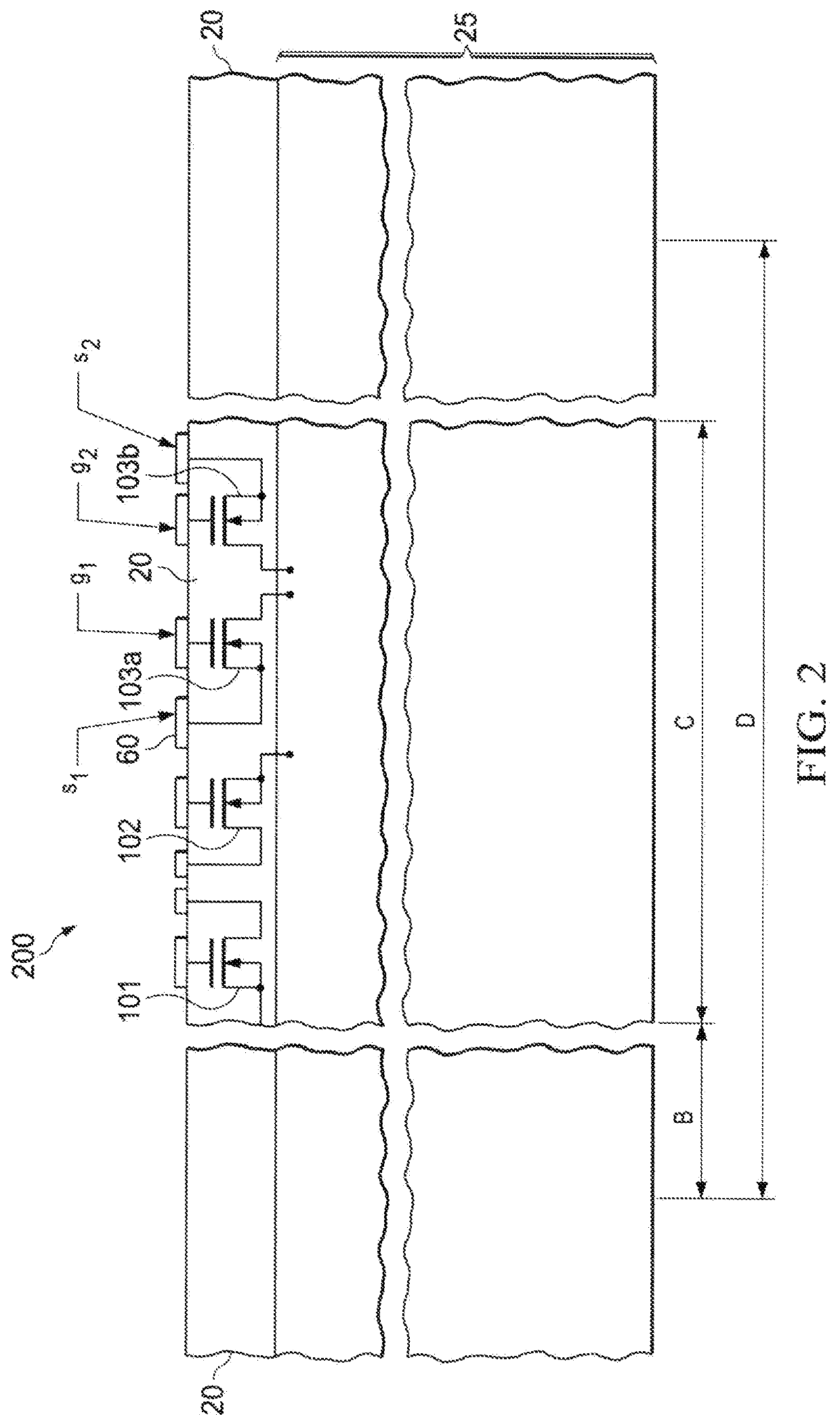
[0035]The silicon chip in this embodiment contains a pair of trench MOSFET devices 103a and 103b. The drain nodes of the two MOSFETs are connected electrically at the back-...


PUM


Abstract

A semiconductor device with reduced device resistance is disclosed. The semiconductor device comprises a semiconductor chip in which the chip thickness at the center portion of the chip where the circuit elements are disposed is uniform and is different from the chip thickness near the chip sides distant from the circuit elements.

Description

BACKGROUND[0001]Semiconductor devices are trending towards thin chips. One reason is the thinning of the final products such as cell phones and flat panel TVs. Also, thin chips perform better in at least two aspects: better heat dissipation and lower power consumption from the reduction of device resistance as the chips get thinner. Semiconductor materials such as silicon have finite electrical resistivity. Electricity flows through it converts power into heat instead of work and is generally undesirable.[0002]One way to reduce device resistance is to build the device with thinner chips. Integrated circuits (ICs) are built in semiconductor wafers of a certain thickness for the physical support of the circuit elements in the wafers. After the front-end processes are complete, the wafer moves to the back-end processes commonly include a back grind step to reduce the wafer thickness before the individual chips are severed from the wafer and packaged. Currently the most advanced wafer t...

Claims


Application Information

Patent Timeline
IPC IPC(8): H01L23/00H01L29/78
CPCH01L24/32H01L29/7802H01L2924/01014H01L2924/13091H01L24/83H01L23/3121H01L25/071H01L23/10H01L29/0657H01L2224/0345H01L2224/05166H01L2224/0346H01L2224/05624H01L2224/05073H01L24/06H01L2224/06181H01L2224/06051H01L2224/05555H01L24/05H01L24/03H01L2224/05558H01L2924/10158H01L2924/00014H01L2924/013H01L2924/01029H01L27/088H01L21/3065H01L21/56
Inventor WILCOXEN, DUANECHUANG, CHIAO-SHUNLIU, RAINTSAI, THOMASZHANG, WILL
Owner DIODES INC
Why Eureka
Try Eureka