Semiconductor Device and Method of Forming the Same

Pending Publication Date: 2022-04-21
UNITED MICROELECTRONICS CORP
View PDF0 Cites 0 Cited by
  • Summary
  • Abstract
  • Description
  • Claims
  • Application Information

AI Technical Summary

Benefits of technology

The present invention provides a semiconductor device with improved element integration by shrinking the cell height of each bit cell. This is achieved by disposing dummy magnetic tunneling junctions (MTJs) in different interconnect layers. A self-aligned merging process is performed to simultaneously define two interconnect layers, thereby improving the sized bottleneck of the original fabricating process. The semiconductor device of the present invention may sufficient reduce the cell height of the bit cell of the semiconductor device under the permissible process window, while maintaining the performance of the whole device.

Problems solved by technology

Nevertheless, most of these products still pose numerous shortcomings such as high chip area, high cost, high power consumption, limited sensibility, and easily affected by temperature variation and how to come up with an improved device to resolve these issues has become an important task in this field.

Method used


Image

  • Semiconductor Device and Method of Forming the Same
  • Semiconductor Device and Method of Forming the Same
  • Semiconductor Device and Method of Forming the Same

Examples


first embodiment

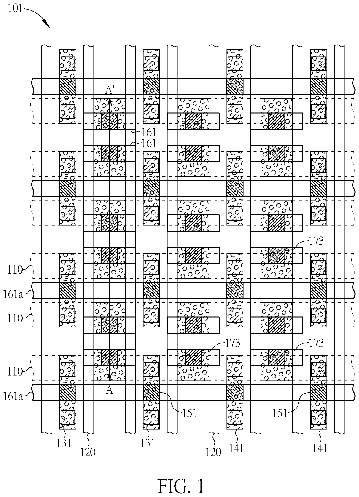
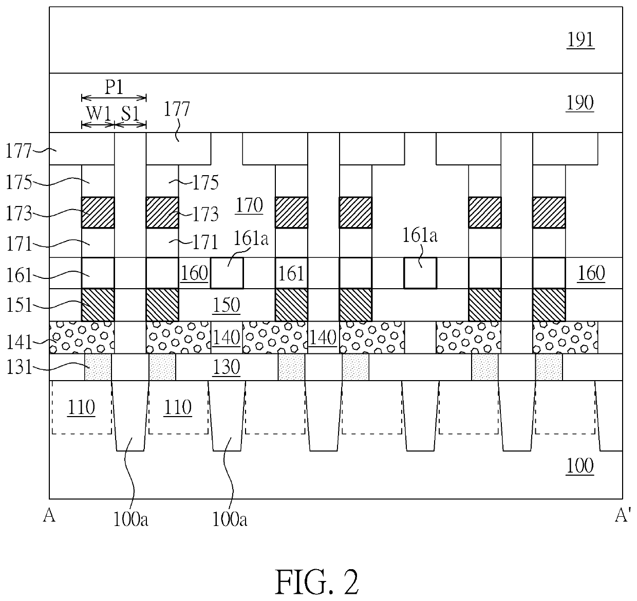
[0028]Please refer to FIGS. 1-2, which illustrate a semiconductor device according to the present invention, wherein FIG. 1 shows a top view of a layout of the semiconductor device and FIG. 2 shows a cross-sectional view of the semiconductor device. The semiconductor device is for example a magnetoresistive random access memory (MRAM) device, and which includes a substrate 100, such as a substrate made of semiconductor material, with the semiconductor material being selected from the group consisting of silicon (Si), germanium (Ge), Si-Ge compounds, silicon carbide (SiC), and gallium arsenide (GaAs). The substrate 100 preferably includes a MRAM region 101 and a logic region (not shown in the drawings) defined thereon. The MRAM region 101 of the substrate 100 further includes a plurality of doped regions (DF) 110, with each of the doped regions 110 being extended along the same direction (such as the x-direction) and spaced from each other by a plurality of shallow trench isolations ...

second embodiment

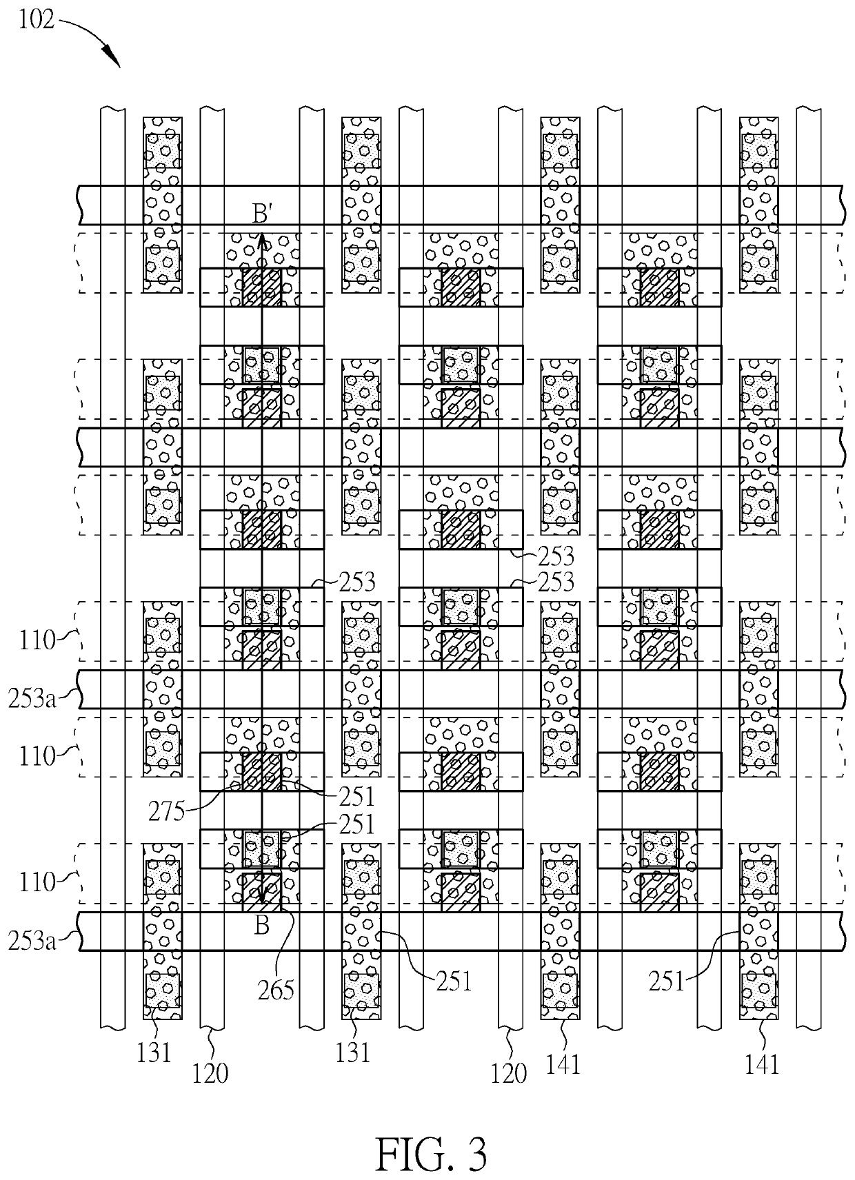
[0036]Please refer to FIG. 3 to FIG. 8, which illustrate a semiconductor device according to the present invention, wherein FIG. 3 shows a top view of a layout of the semiconductor device, FIG. 4 shows a cross-sectional view of the semiconductor device, and FIGS. 5-8 are schematic diagrams showing the fabricating processes of the semiconductor device, respectively. The semiconductor device is for example a MRAM device, and which also includes the substrate 100, the doped regions 110, the shallow trench isolations 100a, the gate structures 120, the plugs 131 disposed within the interlayer dielectric layer 130, the first level metal interconnect layer (for example including the metal interconnections 141 disposed within the inter-metal dielectric layer 140) and the word line 191 disposed within the inter-metal dielectric layer 190. The substrate 100 also includes a MRAM region 102 and the logic region, and all similarities between the aforementioned embodiment and the present embodime...

third embodiment

[0042]Please refer to FIGS. 9-13, which illustrate a semiconductor device according to the present invention, wherein FIG. 9 shows a top view of a layout of the semiconductor device, FIG. 10 shows a cross-sectional view of the semiconductor device, and FIGS. 11-13 are schematic diagrams showing the fabricating processes of the semiconductor device respectively. It order to clearly distinguish the specific layout pattern, not all of the interconnect layers are shown in FIG. 9. The semiconductor device is for example a MRAM device, and which also includes the substrate 100, the shallow trench isolations 100a, the doped regions 110, the gate structures 120, the plugs 131 disposed within the interlayer dielectric layer 130, the second level via conductor layer (for example including the metal interconnections 171), the magnetic memory structures 173, the third level via conductor layer (for example including the metal interconnections 175), the fourth level metal interconnect layer (for...


PUM


Abstract

The present invention provides a semiconductor device and a method of forming the same, and the semiconductor device includes a substrate, a first interconnect layer and a second interconnect layer. The first interconnect layer is disposed on the substrate, and the first interconnect layer includes a first dielectric layer around a plurality of first magnetic tunneling junction (MTJ) structures. The second interconnect layer is disposed on the first interconnect layer, and the second interconnect layer includes a second dielectric layer around a plurality of second MTJ structures, wherein, the second MTJ structures and the first MTJ structures are alternately arranged along a direction. The semiconductor device may obtain a reduced size of each bit cell under a permissible process window, so as to improve the integration of components.

Description

BACKGROUND OF THE INVENTION1. Field of the Invention[0001]The invention relates to a semiconductor device and a method of forming the same, and more particularly to a magnetoresistive random access memory (MRAM) device and a method of forming the same.2. Description of the Prior Art[0002]Magnetoresistance (MR) effect has been known as a kind of effect caused by altering the resistance of a material through variation of outside magnetic field. The physical definition of such effect is defined as a variation in resistance obtained by dividing a difference in resistance under no magnetic interference by the original resistance. Currently, MR effect has been successfully utilized in production of hard disks thereby having important commercial values. Moreover, the characterization of utilizing GMR materials to generate different resistance under different magnetized states could also be used to fabricate MRAM devices, which typically has the advantage of keeping stored data even when th...

Claims


Application Information

Patent Timeline
IPC IPC(8): H01L43/02H01L43/12H01L27/22
CPCH01L43/02H01L27/226H01L43/12H10B61/00H10B61/22H10N50/10H10N50/01H10B61/20H10N50/80H10N50/85
Inventor LEE, KUO-HSINGLIN, CHUN-HSIENHSUEH, SHENG-YUAN
Owner UNITED MICROELECTRONICS CORP
Why Eureka
Try Eureka