Dual clocked synchronous memory device having a delay time register and method of operating same

a delay time register and synchronous memory technology, applied in the direction of memory adressing/allocation/relocation, generating/distributing signals, instruments, etc., can solve the problems of not all interface signals are bused, no multiple processing elements, no ability for multiple outstanding requests,

Inactive Publication Date: 2000-03-07
RAMBUS INC
View PDF41 Cites 134 Cited by
  • Summary
  • Abstract
  • Description
  • Claims
  • Application Information

AI Technical Summary

Problems solved by technology

Prior art memory systems have attempted to solve the problem of high speed access to memory with limited success.
There are no multiple processing elements and no capability for multiple outstanding requests, and again, not all of the interface signals are bused.
Such packages are difficult to use because of the point-to-point wiring required to interconnect conventional memory devices with processing elements.
No attempt is made to solve the problem by changing the interface.
The clocking scheme used in this invention has not been used before and in fact would be difficult to implement in backplane buses due to the signal degradation caused by connector stubs.

Method used


Image

  • Dual clocked synchronous memory device having a delay time register and method of operating same
  • Dual clocked synchronous memory device having a delay time register and method of operating same
  • Dual clocked synchronous memory device having a delay time register and method of operating same

Examples


Embodiment Construction

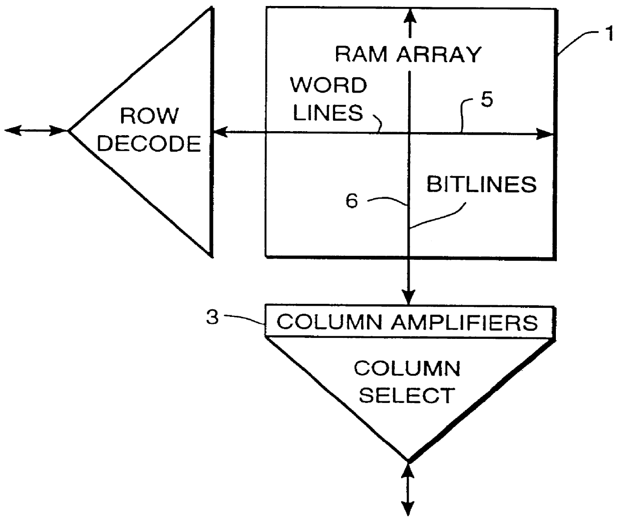
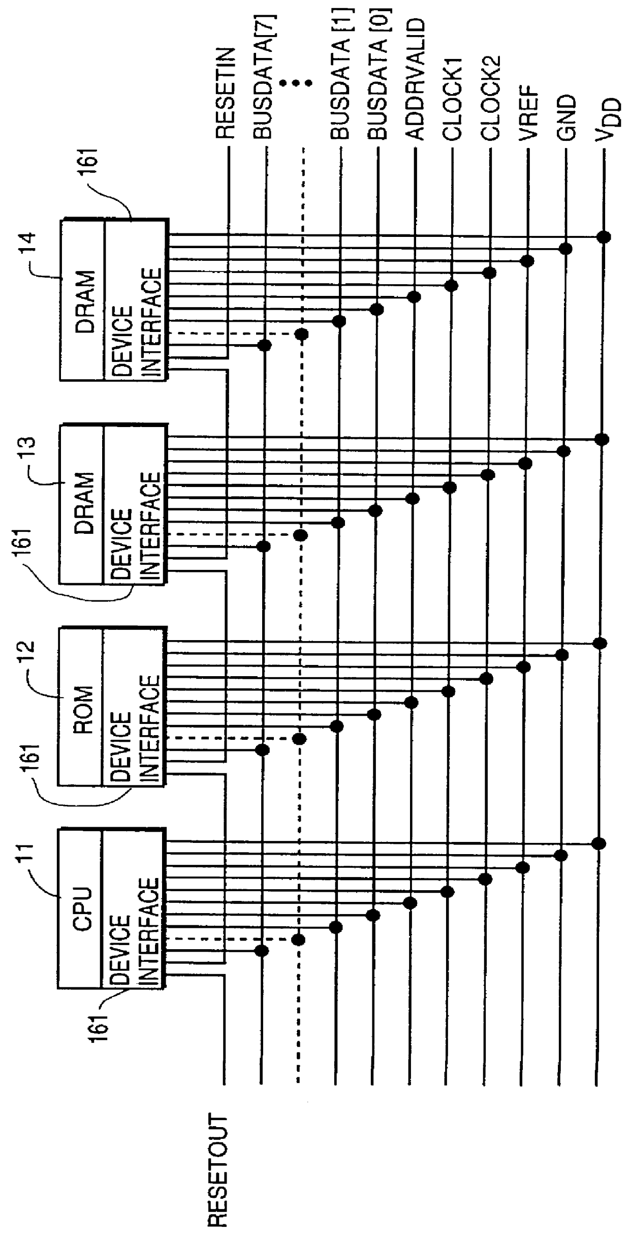
The present invention is designed to provide a high speed, multiplexed bus for communication between processing devices and memory devices and to provide devices adapted for use in the bus system. The invention can also be used to connect processing devices and other devices, such as I / O interfaces or disk controllers, with or without memory devices on the bus. The bus consists of a relatively small number of lines connected in parallel to each device on the bus. The bus carries substantially all address, data and control information needed by devices for communication with other devices on the bus. In many systems using the present invention, the bus carries almost every signal between every device in the entire system. There is no need for separate device-select lines since device-select information for each device on the bus is carried over the bus. There is no need for separate address and data lines because address and data information can be sent over the same lines. Using the...


PUM


Abstract

A synchronous memory device having at least one memory section which includes a plurality of memory cells. The memory device comprises a register to store a value which is representative of a delay time after which the memory device responds to a read request and clock receiver circuitry to receive first and second external clock signals. The memory device also includes an output driver(s) to output data on a bus, in response to a read request and in accordance with the delay time, wherein a first portion of the data is output synchronously with respect to the first external clock signal and a second portion of the data is output synchronously with respect to the second external clock signal. The memory device may include a delay locked loop to generate internal clock signal(s) using the external clock signal(s). The output drivers output data on the bus in response to the internal clock signal(s). The memory device may include input receiver circuitry, coupled to the bus, the receive the read request, wherein the read request is sampled from the bus synchronously with respect to the first external clock signal.

Description

FIELD OF THE INVENTIONAn integrated circuit bus interface for computer and video systems is described which allows high speed transfer of blocks of data, particularly to and from memory devices, with reduced power consumption and increased system reliability. A new method of physically implementing the bus architecture is also described.BACKGROUND OF THE INVENTIONSemiconductor computer memories have traditionally been designed and structured to use one memory device for each bit, or small group of bits, of any individual computer word, where the word size is governed by the choice of computer. Typical word sizes range from 4 to 64 bits. Each memory device typically is connected in parallel to a series of address lines and connected to one of a series of data lines. When the computer seeks to read from or write to a specific memory location, an address is put on the address lines and some or all of the memory devices are activated using a separate device select line for each needed d...

Claims


Application Information

Patent Timeline
Patent Type & Authority Patents(United States)
IPC IPC(8): G06F12/06G06F13/36G06F12/02G06F13/376G06F13/16G11C11/409G11C11/4096G11C7/10G11C5/06G11C8/00G11C11/4076G11C7/22G11C11/407G11C7/00G11C5/00G11C29/00G06F11/10G06F11/00G06F1/10G06F12/00G11C11/401
CPCG06F11/006G06F12/0215G06F12/0661G06F12/0684G06F13/1605G06F13/161G06F13/1678G06F13/1689G06F13/1694G06F13/376G06F13/4239G11C5/00G11C5/04G11C5/06G11C5/063G11C5/066G11C7/1006G11C7/1012G11C7/1045G11C7/1051G11C7/1057G11C7/1066G11C7/1069G11C7/1072G11C7/1078G11C7/1084G11C7/22G11C7/222G11C7/225G11C8/00G11C11/4076G11C11/4096G11C29/88Y02B60/1235G11C2207/105G11C2207/108Y02B60/1225Y02B60/1228G06F11/1048Y02D10/00
Inventor FARMWALD, MICHAELHOROWITZ, MARK
Owner RAMBUS INC
Why Eureka
Try Eureka