Self-biasing CMOS PECL receiver with wide common-mode range and multi-level-transmit to binary decoder

a binary decoder and receiver technology, applied in the direction of logic circuits using specific components, logic circuit coupling/interface arrangement, pulse technique, etc., can solve the problems of less responsiveness of receivers, less power required, and inability to respond to bicmos fast, so as to simplify interconnect routing and reduce power

Inactive Publication Date: 2000-04-11
DIODES INC
View PDF8 Cites 103 Cited by
  • Summary
  • Abstract
  • Description
  • Claims
  • Application Information

AI Technical Summary

Benefits of technology

Only one voltage reference is needed, even for multi-level inputs having three voltage levels. The fact that the differential inputs are complements of each other is exploited to eliminate the second voltage reference. Both of the differential inputs are compared to a single threshold, using a single voltage-reference. Using

Problems solved by technology

Although BiCMOS is fast, it is also more expensive than standard CMOS.
However, as the change in input voltages increases, some receivers are less responsive and may even fail.
Thus, receivers often have a limited common-mode range.
Unfortunately, that receiver uses a bi-stable amplifier, which can be temperamental.
However, the range is still somewhat limited, as eventually differential n-channel transistors 26, 28 turn off as the common-mode input voltage is reduced to around 1 volt above ground.
While such MLT-to-binary decoders are useful, having two voltage references is undesirable.
When

Method used


Image

  • Self-biasing CMOS PECL receiver with wide common-mode range and multi-level-transmit to binary decoder
  • Self-biasing CMOS PECL receiver with wide common-mode range and multi-level-transmit to binary decoder
  • Self-biasing CMOS PECL receiver with wide common-mode range and multi-level-transmit to binary decoder

Examples


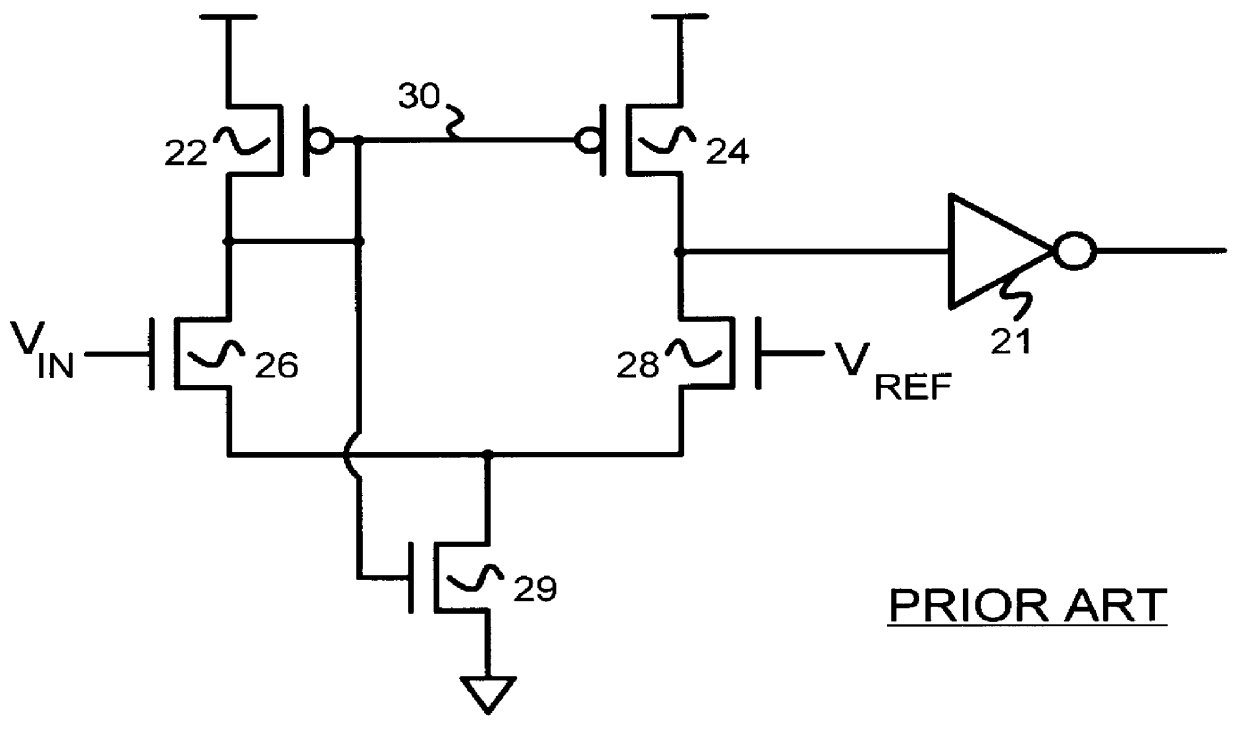
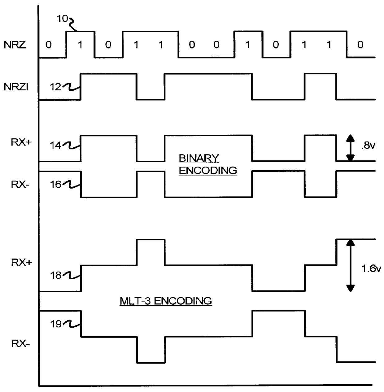
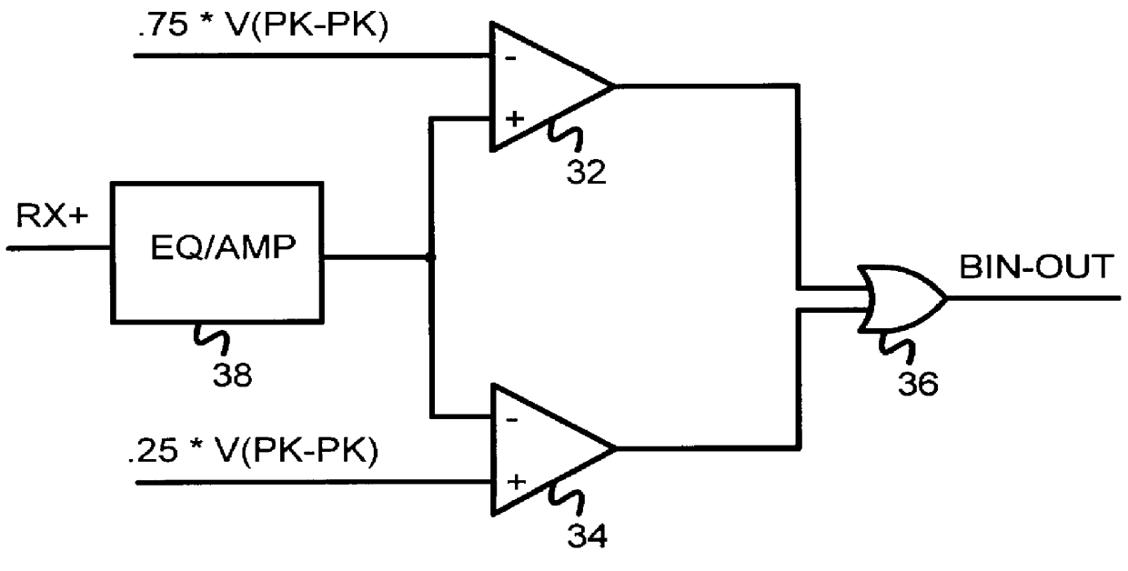
Embodiment Construction

Several other embodiments are contemplated by the inventors. For example other kinds of encoding of data streams may be substituted. More complex multi-level-transition inputs may be used having more than three levels. When more levels are used, variations between the voltage references become more critical. The invention can still reduce the number of voltage references required for these more complex input signals, making more complex multi-level schemes feasible. The voltage-reference generator can be expanded to generate additional voltage references and select one or more of these references using additional resistors in the voltage divider and additional transmission gates for selection. Additional self-biased comparators can be used in parallel for additional comparisons with the additional voltage references. More complex decoding logic may be used than the simple OR gate described.

The foregoing description of the embodiments of the invention has been presented for the purpo...


PUM


Abstract

A pseudo-emitter-coupled-logic (PECL) receiver has a wide common-mode range. Two current-mirror CMOS differential amplifiers are used. One amplifier has n-channel differential transistors and a p-channel current mirror, while the second amplifier has p-channel differential transistors and an n-channel current mirror. When the input voltages approach power or ground, one type of differential transistor continues to operate even when the other type shuts off. The outputs of the two amplifiers are connected together and each amplifier receives the same differential input signals. The tail-current transistor is self-biased using the current-mirror's gate-bias. This self biasing of each amplifier eliminates the need for an additional voltage reference and allows each amplifier to adjust its biasing over a wide input-voltage range. Thus the common-mode input range is extended using self biasing and complementary amplifiers. The complementary self-biased comparators can be used for receiving binary or multi-level-transition (MLT) inputs by selecting different voltage references for threshold comparison. Using the same reference on both differential inputs eliminates a second reference for multi-level inputs having three levels. Thus binary and MLT inputs can be detected and decoded by the same decoder.

Description

BACKGROUND OF THE INVENTION--FIELD OF THE INVENTIONThis invention relates to a CMOS self-biased comparator, and more particularly to a pseudo-ECL receiver and a binary-to-multi-level-transition (MLT-3) decoder each using the CMOS self-biased comparator.BACKGROUND OF THE INVENTION--DESCRIPTION OF THE RELATED ARTHigh-speed communications networks such as Fast (100 Mbps) Ethernet and asynchronous-transfer-mode (ATM) networks use differential signals for transmitting data. The speed of these differential signals is increased when they transition over a reduced voltage range, since output capacitances are charged and discharged over a smaller voltage range, requiring less current.Small-signal differential drivers and differential amplifiers are needed for these network applications. In the past, bipolar NPN transistors arranged as emitter-coupled-logic (ECL) gates were used. However, complementary metal-oxide-semiconductor (CMOS) is a less expensive technology than bipolar. Bipolar NPN t...

Claims


Application Information

Patent Timeline
IPC IPC(8): H03K19/0185H03K19/0175
CPCH03K19/018528
Inventor MANOHAR, AMAR S.LEE, BOR
Owner DIODES INC
Why Eureka
Try Eureka