Power transistor having vertical FETs and method for making same

a vertical fet, power transistor technology, applied in the direction of transistors, electrical devices, semiconductor devices, etc., can solve the problems of difficult to achieve geometries and channel length control required to achieve the desired objectives, inconvenient operation, and inconvenient operation

Inactive Publication Date: 2000-05-09
IBM CORP
View PDF5 Cites 89 Cited by
  • Summary
  • Abstract
  • Description
  • Claims
  • Application Information

AI Technical Summary

Problems solved by technology

Furthermore, inter-electrode capacitance, lead inductance and carrier transit time limit the maximum frequency of operation.
Geometries and channel length control required for achieving the desired objectives have been difficult to attain in conventional silicon devices using such planar transistors.
The planar transistors have relatively large surface area requirements and have developed operational problems in sub-micron integrated c

Method used


Image

  • Power transistor having vertical FETs and method for making same
  • Power transistor having vertical FETs and method for making same
  • Power transistor having vertical FETs and method for making same

Examples


Embodiment Construction

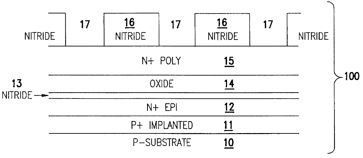
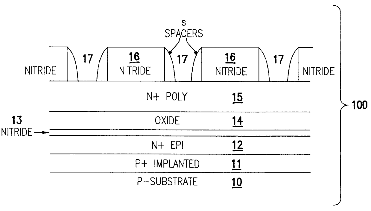
Referring now to the drawings, there is shown a representative portion of a power transistor structure made according to the method of the present invention in enlarged views at several stages of the fabrication scheme.

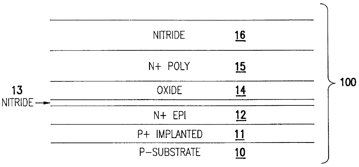
Referring to FIG. 1, a structure suitable for starting preparation of a power transistor 100 is depicted including a substrate 10, which has surface and a first conductivity type. As exemplified, the substrate 10 is a P-type single crystal silicon wafer 10.

A heavily doped P+ layer 11 is formed across the surface of wafer 10 by implanting boron ions in the surface of the wafer 10. For example, borons ions can be implanted at a peak concentration of greater than 10.sup.20 ions cm.sup.-3 (10.sup.15 to 10.sup.16 cm.sup.-2) at 10-100 keV. This P+ layer 11 will serve as an an etch stop layer during a later described step of thinning the backside of the transistor structure under fabrication.

An N+ layer 12 is then epitaxially grown on the surface of P+ layer 11. Conventiona...


PUM


Abstract

A power transistor having of a plurality of vertical MOSFET devices combined in parallel to achieve high-performance operation and methods of fabricating this device.

Description

1. Field of the InventionThe invention relates to a power transistor and methods for its fabrication.2. Description of the Related ArtHigh-performance power amplifiers and switching devices require low on-resistance, i.e., low resistance during conduction of current by the device, to limit internal power dissipation at high levels of operating current. For low voltage power supply applications, ultra-low on-resistance is essential. Furthermore, inter-electrode capacitance, lead inductance and carrier transit time limit the maximum frequency of operation. Additionally, power devices must efficiently dissipate internally generated heat. With the expanding market for high power communications amplifiers and switching applications (e.g., automotive, mechanical control), there is an increased need for high-performance, low-voltage, inexpensive, solid-state power devices.Conventional power MOSFETs used in these devices and applications employ planar transistors. Geometries and channel len...

Claims


Application Information

Patent Timeline
IPC IPC(8): H01L21/02H01L29/66H01L21/336H01L29/40H01L29/423H01L29/78
CPCH01L29/7827H01L29/66666H01L21/2255
Inventor BERTIN, CLAUDE L.GAMBINO, JEFFREY P.MANDELMAN, JACK A.
Owner IBM CORP
Why Eureka
Try Eureka