Shallow trench isolation for semiconductor devices

a technology for semiconductor devices and trenches, applied in semiconductor/solid-state device manufacturing, basic electric elements, electric devices, etc., can solve the problems of poor quality gate oxide sometimes formed over shoulder regions 38, difficult to effectively implement the structure of the locos field isolation, and insufficient device isolation over their entire width

Inactive Publication Date: 2000-05-30
UNITED MICROELECTRONICS CORP
View PDF6 Cites 61 Cited by
  • Summary
  • Abstract
  • Description
  • Claims
  • Application Information

AI Technical Summary

Problems solved by technology

The LOCOS technique has various drawbacks, however, including its well known problems related to stress generation and the thin "bird's beak" region formed at the periphery of the LOCOS field isolation structure.
Particularly because of the bird's beak problem, the LOCOS field isolation structure is difficult to implement effectively for small device geometries and so must be replaced in high density devices by a more readily scaled device isolation structure.
In this regard, shallow trench isolation structures are unlike LOCOS isolation regions, which must accommodate the bird's beak structures on either side of the LOCOS isolation region and so do not provide device isolation over their entire width.
Thus, the poor quality gate oxide sometimes formed over shoulder regions 38 is sufficiently thin and poor as to allow for parasitic MOSFET action at the shoulder region.

Method used


Image

  • Shallow trench isolation for semiconductor devices
  • Shallow trench isolation for semiconductor devices
  • Shallow trench isolation for semiconductor devices

Examples


Embodiment Construction

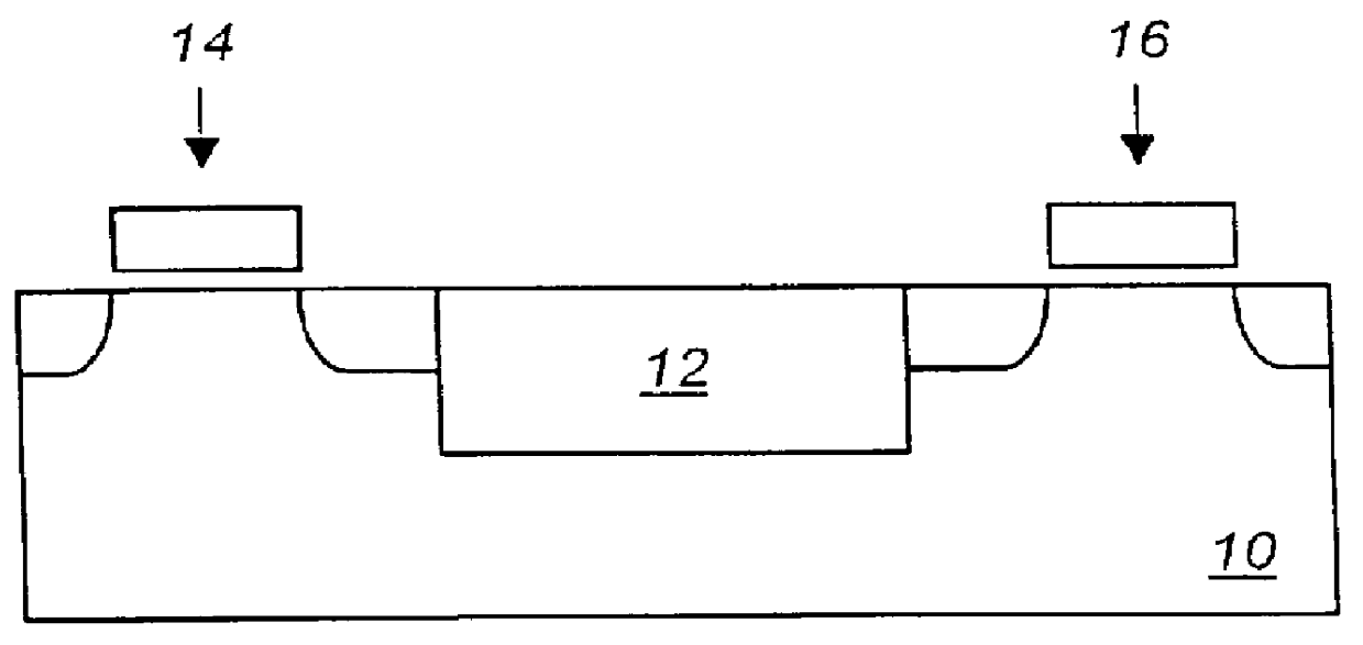
In accordance with a first aspect of the present invention, an integrated circuit device is formed by etching a trench into a substrate which has portions of the substrate adjacent the trench doped to a first conductivity type. The trench is coated with a layer of doped dielectric material and the dopants from the doped dielectric material are diffused into the substrate to form self-aligned doping regions along the walls of the trench. The isolation doping region and the trench together form a device isolation structure for the integrated circuit device.

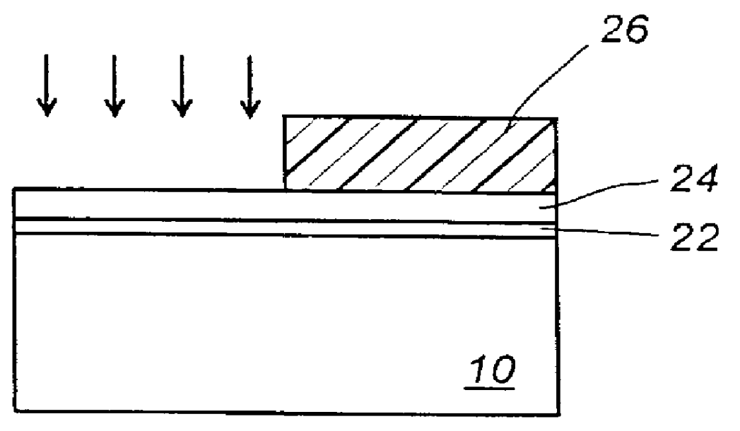
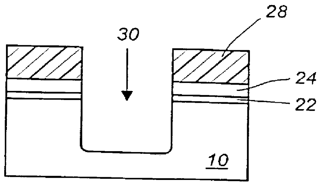
Another aspect of the invention provides a method of forming an integrated circuit device on a substrate having at least a surface doped to a first conductivity type. A trench definition mask is provided over the substrate and the substrate is etched through the trench definition mask to form a trench in the substrate. A first dielectric layer doped with first dopants is deposited over the substrate and within the trench. A second d...


PUM


Abstract

A shallow trench isolation structure is formed by providing a pad layer and a silicon nitride polish stop layer on a surface of a P-type silicon substrate. The silicon nitride polish stop layer and the pad oxide layer are patterned to define openings corresponding to portions of the substrate that will be etched to form trenches. Trenches are defined in the P-type silicon substrate by anisotropic etching. A boron doped oxide or glass is deposited along the walls and floor of the trench. An undoped TEOS oxide is provided over the doped oxide or glass to complete filling of the trench. The device is subjected to a high temperature reflow process, causing the dielectric materials to flow, partially planarizing the device and causing the boron of the first layer to diffuse into the walls and floor of the trench. Chemical mechanical polishing removes excess portions of the dielectric layers. The silicon nitride polish stop layer and the pad oxide layer are removed and conventional processing is performed to complete devices on the substrate. Diffusion of boron into the walls of the trench forms a self-aligned field doping region for the shallow trench isolation structure using relatively few processing steps.

Description

1. Field of the InventionThe present invention relates to the provision of isolation structures between devices of an integrated circuit formed in and on a semiconductor substrate and, more particularly, to the formation of shallow trench isolation structures.2. Description of the Related ArtA variety of integrated circuits incorporate device isolation structures formed between adjacent semiconductor devices to prevent carriers from traveling through the substrate between the adjacent devices. For example, device isolation structures are conventionally formed between adjacent field effect transistors (FETs) in dense semiconductor circuits such as dynamic random access memories (DRAMs) to reduce charge leakage to and from the charge storage nodes of the FETs. Often, device isolation structures take the form of thick field oxide regions extending below the surface of the semiconductor substrate. The most common early technique for forming a field oxide region is the local oxidation of...

Claims


Application Information

Patent Timeline
Patent Type & Authority Patents(United States)
IPC IPC(8): H01L21/762H01L21/70
CPCH01L21/76237
Inventor HONG, GARY
Owner UNITED MICROELECTRONICS CORP
Why Eureka
Try Eureka