

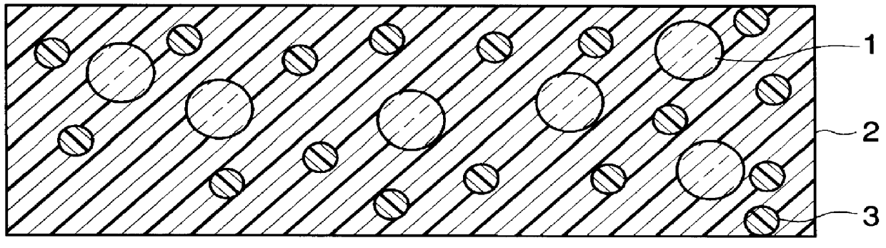
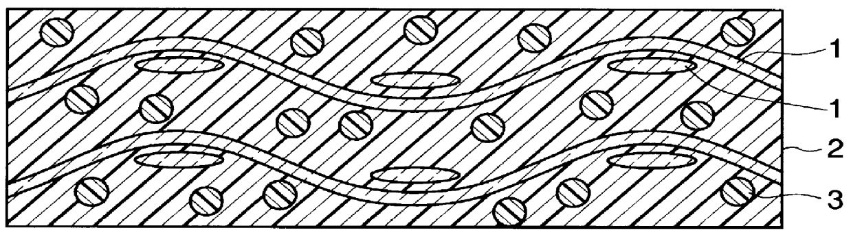
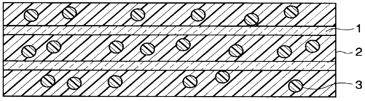
Laminate and multilayer printed circuit board
a printed circuit board and laminate technology, applied in weaving, semiconductor/solid-state device details, other domestic articles, etc., can solve the problems of enlarging the elastic modulus of the substrate, affecting the stability of the substrate,
- Summary
- Abstract
- Description
- Claims
- Application Information
AI Technical Summary
Benefits of technology
Problems solved by technology
Method used
Image

Examples
example 1
88 parts (by weight) of phenol-novolak resin (trade name "XL225-3L", produced by Mitsui Toatsu Chamicals, Inc.) as a setting agent and 10 parts (by weight) of amine-modified dimethylsiloxane ("PS51311", Chisso Corporation) as a component of low elastic modulus were added to 100 parts (by weight) of epoxy compound ("EXA-1514", Dai-Nippon Ink and Chamicals, Inc.) in methyl ethyl ketone. Thus, a varnish which had a solid matter content of 50 (weight-%) was prepared. A piece of E-glass (electrical glass) cloth 100 (.mu.m) thick was impregnated and coated with the varnish, and then dried at 120 (.degree.C.) for 10 (min) so as to remove the solvent. Thus, a piece of prepreg was obtained. The resin content of the obtained prepreg was 70 (weight-%).
Copper foils (each being 18 (.mu.m) thick) were respectively superposed on both the surfaces of the obtained prepreg, and the resulting structure was pressed under heat by a press. Thus, a laminate was obtained. AS pressing conditions on this occ...
example 2
Resin components were prescribed in such a way that 55 parts (by weight) of phenol-novolak (trade name "H100", produced by Hitachi Chemical Co., Ltd.) as a setting agent and 15 parts (by weight) of epoxy-modified polydimethylsiloxane ("SF8413", Toray Silicone Co., Ltd.) as a component of low elastic modulus were added to 100 parts (by weight) of epoxy compound ("YX4000H", Yuka Shell Kabushiki-Kaisha). On this occasion, the setting agent and the component of low elastic modulus were reacted at 90 (.degree.C.) for 30 (min) in methyl isobutyl ketone beforehand as a pre-reaction, and the resulting solution was cooled down to room temperature. Thereafter, the epoxy compound was added into the cooled solution. Thus, a varnish which had a solid matter content of 50 (weight-%) was prepared. A piece of S-glass (structural glass) cloth 70 (.mu.m) thick was impregnated and coated with the prepared varnish, and then dried at 140 (.degree.C.) for 10 (min) so as to remove the solvent Thus, a piec...
example 3
Resin components were prescribed as consisting of 100 parts (by weight) of maleimide compound (bis(4-maleimidophenyl) methane, produced by Mitsui Toatsu Chamicals, Inc.), 38 parts (by weight) of amine compound (2, 2-bis(4-(4-aminophenoxy) phenyl) propane, Wakayama Fine Chemical Co.) and 5 parts (by weight) of amine-modified polydimethyleiloxane (trade name "SF84181", Toray Silicone Co., Ltd.). On this occasion, pre-reactions were so performed that 50 parts (by weight) of the maleimide compound and the amine-modified polydimethylsiloxane were reacted in dimethylformamide at 110 (.degree.C.) for 20 (min), and that the remaining 50 parts (by weight) of the maleimide compound and the amine compound were added into the resulting solution and were reacted for 20 (min). Thus, a varnish which had a solid matter content of 40 (weight-%) was prepared. Further, 20 parts (by weight) of fused silica filler (at an average grain diameter of 10 (.mu.m)) were mixed and dispersed into the prepared va...
PUM
| Property | Measurement | Unit |
|---|---|---|
| glass transition temperature | aaaaa | aaaaa |
| weight | aaaaa | aaaaa |
| clock frequency | aaaaa | aaaaa |
Abstract
Description
Claims
Application Information