Method of fabricating an integrated complex-transition metal oxide device

a metal oxide device and complex-transition technology, applied in the direction of semiconductor devices, basic electric elements, electrical equipment, etc., can solve the problems of complex-transition metal oxide devices that are difficult to integrate with the standard processing techniques used, and the process requirements for growing high-quality complex-transition metal oxide films typically conflict with the requirements used for producing integrated devices

Inactive Publication Date: 2000-09-05
NORTHEASTERN UNIV
View PDF35 Cites 90 Cited by
  • Summary
  • Abstract
  • Description
  • Claims
  • Application Information

AI Technical Summary

Problems solved by technology

However, their novel properties derive from complex crystallographic structures that heretofore have been difficult to integrate with the standard processing techniques used by the electronics, photonics and MEMS communities.
Unfortunately, it has thus far been difficult to integrate complex-transition metal oxide devices with current processes, where here integration is denoted as being able to fabricate both complex-transition metal oxide devices and semiconductor-based devices on the same substrate material using methods compatible with semiconductor batch processing techniques.
Unfortunately, the process requirements needed for growing high quality complex-transition metal oxide films typically conflicts with the requirements used for producing integrated devices.
Moreover, the problems that beset integrating complex-transition metal oxide films with standard semiconductor fabrication techniques also hold for some intermetallic alloy systems that also have large chemical formulas and complex unit cells, and possess long ranged cooperative phenomenon.
Unfortunately, garnet films deposited at temperatures of 500.degree. C. are structurally amorphous, and show no useful ferrimagnetic properties.
This procedure can still degrade the properties of other materials on the wafer unless great care is taken in the ordering of the total wafer fabrication process.
Despite the hard-won successes of the direct film deposition technique, the resulting complex-transition metal oxide films do not necessarily possess optimal material properties since they are polycrystalline, and not structurally highly-oriented or single-crystal.
For most applications involving complex transition-metal oxide films, devices made with polycrystalline films have reduced performance or increased losses compared to single-crystal films.
For example, devices made from polycrystalline ferrimagnetic films will have higher magnetic loss compared to the same device made from a single-crystal film, while any imperfections in a high-temperature superconducting film will reduce its current carrying capacity.
For example, it is known that during the growth of many CTMO films by vapor phase deposition techniques slight changes in the film stoichiometry through oxygen-deficiency will cause the formation of dislocation sites, which in turn promote high stress at the film / substrate interface.

Method used


Image

  • Method of fabricating an integrated complex-transition metal oxide device
  • Method of fabricating an integrated complex-transition metal oxide device
  • Method of fabricating an integrated complex-transition metal oxide device

Examples


Embodiment Construction

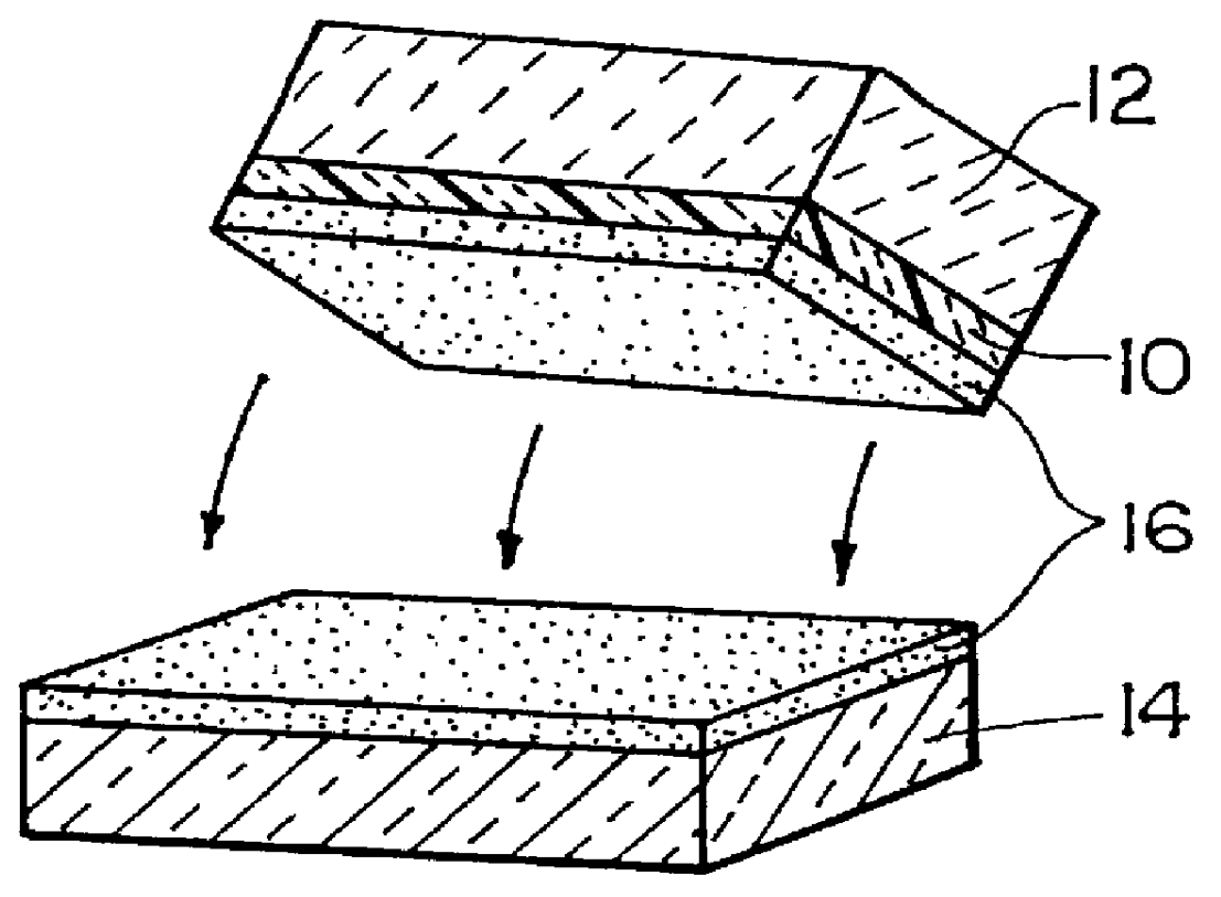
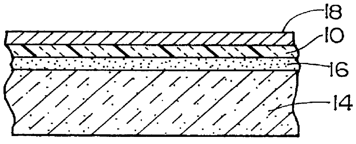
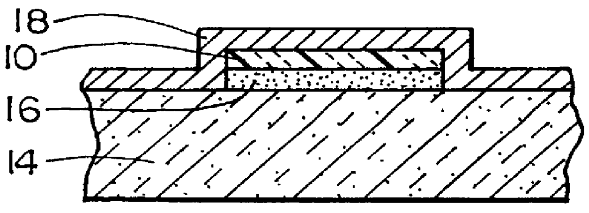
One example for the use of the present invention involves the fabrication of integrated single-crystal yttrium iron garnet circulators on a metallized silicon substrate 14 at low temperatures. Single-crystal yttrium iron garnet (often denoted as YIG) films 10, having thicknesses over 100 micrometers, can be routinely grown on lattice-matched gadolinium gallium garnet (often denoted as GGG) substrates 12 by liquid phase epitaxy, but have never been grown on semiconductor substrates 14. As discussed previously, integrated polycrystalline garnet / semiconductor circulators have been produced through the direct fabrication method at using processing temperatures above 700.degree. C. However, integrated single-crystal garnet circulators have performance benefits over integrated polycrystalline garnet circulators, and there is a greatly reduced risk of degrading the device characteristics if the integration is done at low temperatures.

An integrated single-crystal YIG / silicon circulator was ...


PUM

PropertyMeasurementUnit
thicknessesaaaaaaaaaa
temperatureaaaaaaaaaa
frequencyaaaaaaaaaa

Abstract

A method for the fabrication complex-transition metal oxide (CTMO)/semiconductor or dielectric substrate integrated devices includes the separation of the CTMO film growth process from the CTMO-film/semiconductor or dielectric substrate integration process. The CTMO-film is transferred from the native substrate to the final substrate for fabrication into devices. The CTMO-film is grown onto a native substrate under growth conditions chosen to provide a CTMO-film having desirable properties and thickness. No restrictions are placed upon the native substrate used, the growth method used, or on the growth conditions required. The CTMO-film is then joined to the semiconductor or dielectric substrate and the native substrate is removed, providing the basis for an integrated electronics, photonics, or MEMS device. Techniques fully compatible with semiconductor processing can be used to fabricate monolithically integrated CTMO/semiconductor devices in a first embodiment.

Description

Not ApplicableBACKGROUND OF THE INVENTIONComplex-transition metal oxides comprise a large group of materials that show an extremely diverse and useful range of characteristics. Examples of but a few technologically useful complex-transition metal oxide materials include ferrimagnetic materials having the spinel, garnet, or hexaferrite crystallographic structures, ferroelectric materials having the perovskite crystallographic structure, and perovskites that display superconducting behavior at liquid nitrogen temperatures. All of these examples are of note because they are both of great technological interest as well as manifestations for the presence of long range cooperative order in the materials. Because of their potential impact on modern electronics, photonics, and microelectromechanical systems (MEMS) applications they are being intensively researched. However, their novel properties derive from complex crystallographic structures that heretofore have been difficult to integrat...

Claims


Application Information

Patent Timeline
Patent Type & Authority Patents(United States)
IPC IPC(8): C04B41/81H01L21/02H01L21/20
CPCC04B41/81H01L21/2007H01L2221/68359H01L2221/68363H01L2221/68368
Inventor OLIVER, STEVEN A.ZAVRACKY, PAULMCGRUER, NICOL E.VITTORIA, CARMINE
Owner NORTHEASTERN UNIV
Why Eureka
Try Eureka