Dynamic random access memories with dielectric compositions stable to reduction

a dielectric composition and random access technology, applied in the field of memory devices, can solve the problems of increasing processing difficulties, unacceptably high leakage current, and rapidly approaching the capacitance per unit area limit of the second phase of the capacitor

Inactive Publication Date: 2000-10-31
SHARP KK
View PDF10 Cites 21 Cited by
  • Summary
  • Abstract
  • Description
  • Claims
  • Application Information

AI Technical Summary

Problems solved by technology

However, SiO.sub.2 is quickly approaching its capacitance per unit area limit, as further decreases in the thickness will eventually lead to an unacceptably high leakage current and increasing processing difficulties.
However, one of the primary reliability problems that may preclude the use of these materials

Method used


Image

  • Dynamic random access memories with dielectric compositions stable to reduction

Examples


Embodiment Construction

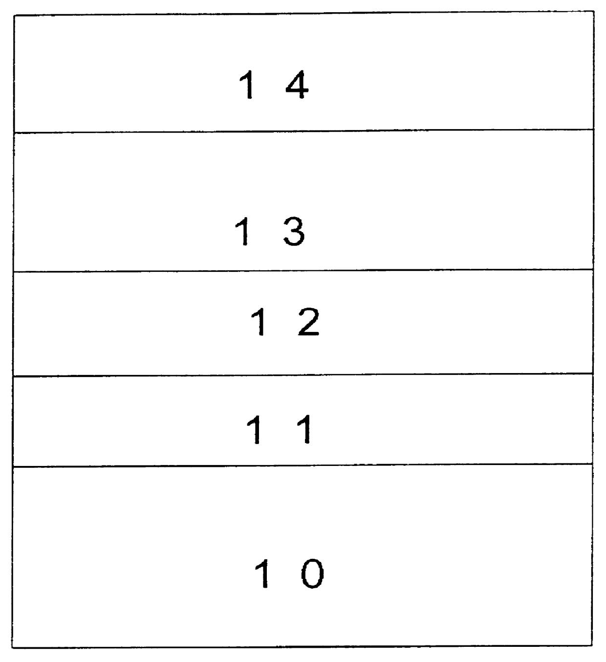
Referring to the FIGURE, a dielectric capacitor device is shown according to one embodiment of the invention. A substrate (10) has the bottom electrode (12) deposited on it to act as a conductor for making connection to other circuit elements in the integrated circuit. The substrate (10) in most cases is a layer of silicon dioxide over a silicon chip. Of course, the substrate may also be bare silicon, gallium arsenide or a multilayer structure having various circuit elements in a silicon chip having layers of silicon dioxide, polysilicon, implanted silicon layers etc. to form what is referred to as a complex integrated circuit. A layer (11) is formed between the substrate (10) and the bottom electrode structure (12) for adhesion and / or diffusion barrier purposes. Thus it provides the necessary adhesion for the metal to the underlying substrate material. The electrode layer (12) is usually a metal such as Rh, Ir, Ru, Os, Pt, Re etc. (transition metals) or an alloy of one or more of t...


PUM

PropertyMeasurementUnit
Dielectric polarization enthalpyaaaaaaaaaa
Compositionaaaaaaaaaa

Abstract

A charge storage device is resistant to degradation in reducing atmospheres for use in dynamic random access memories. The device consists of a dielectric layer that is sandwiched between two electrodes and grown on a suitable substrate such as silicon or silicon coated with silicon dioxide. The dielectric layer is either (a) a modified composition of BaxSr1-xTiO3, 0<x<1 (BST) doped with acceptor type dopants such as Mn, Co, Mg, Cr, Ga and Fe ions as the dielectric layer in the capacitor; the acceptor ions can occupy the titanium sites to prevent the formation of Ti3+ and inhibit the formation of conductive BST by compensating the charges of the oxygen vacancies, and by trapping the free electrons more freely than Ti4+, or (b) modified dielectric compositions with alkaline-earth ions with compositions [(BaxMx)O]yTiO2 (where M can be Ca, Sr or Mg) with the value of y slightly larger than unity.

Description

1. Field of the InventionThis invention relates to memory devices, and more particularly to a memory device such as a dynamic random access memory (DRAM) that has dielectric compositions stable or resistant to H.sub.2 and other anneal treatments and is stable to a reducing atmosphere.2. Description of Related ArtSince its introduction more than three decades ago, the dynamic random access memory has been successfully adopted as a device to store information in the form of charge [see L. H. Parker and A. F. Tasch, IEEE Devices and Circuit Magazine, January 1990, p. 17]. One of the more popular configurations for the memory cells in these devices involves a single capacitor in which charge is stored, and a single transistor that is used to isolate the capacitor. Over the years, as the number of memory cells has been increased from 4 kilobits (kb) in the original designs to Megabit (Mb) levels in the current designs, there has been a constant reduction in the available area per memory ...

Claims


Application Information

Patent Timeline
IPC IPC(8): C04B35/47C04B35/462C04B35/468H01L21/02H01L21/316C04B35/46H01G4/33H01L21/822H01L21/8242H01L21/8246H01L27/04H01L27/10H01L27/105H01L27/108
CPCC04B35/4682H01L28/55H01L21/31691C04B35/47H01L21/02197H01L21/02304C04B35/00C04B35/468
Inventor DESU, SESHU B.SUCHICITAL, CARLOS A.VIJAY, DILIP P.
Owner SHARP KK
Why Eureka
Try Eureka