Although IDDQ testing has been used effectively on
CMOS integrated circuits (ICs) with submicron feature sizes (integrated circuits utilizing dimensions less than 1 .mu.m), its effectiveness on ICs scaled to the deep submicron regime (typically L.sub.effective <0.5 .mu.m) has not been studied extensively.
This is due to increased
circuit complexity and circuit densities, and reduced circuit feature sizes.
In addition, a greater emphasis must be placed on implementing design-for-test (DFT) strategies early in the
design cycle due to the heavy burden and costs associated with back-of-the-line testing.
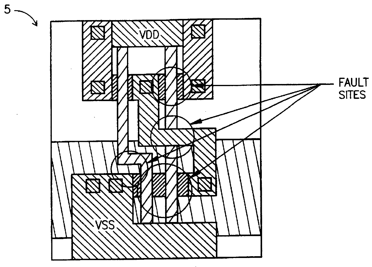
This is significant since physical defects and parametric variations such as
hot electrons, gate induced drain leakage (GIDL), and excessive subthreshold leakage result in increased quiescent current.
This is especially true since some types of defects are difficult to detect using conventional commercial tools.
These are low current defects which can cause catastrophic
system failure if undetected.
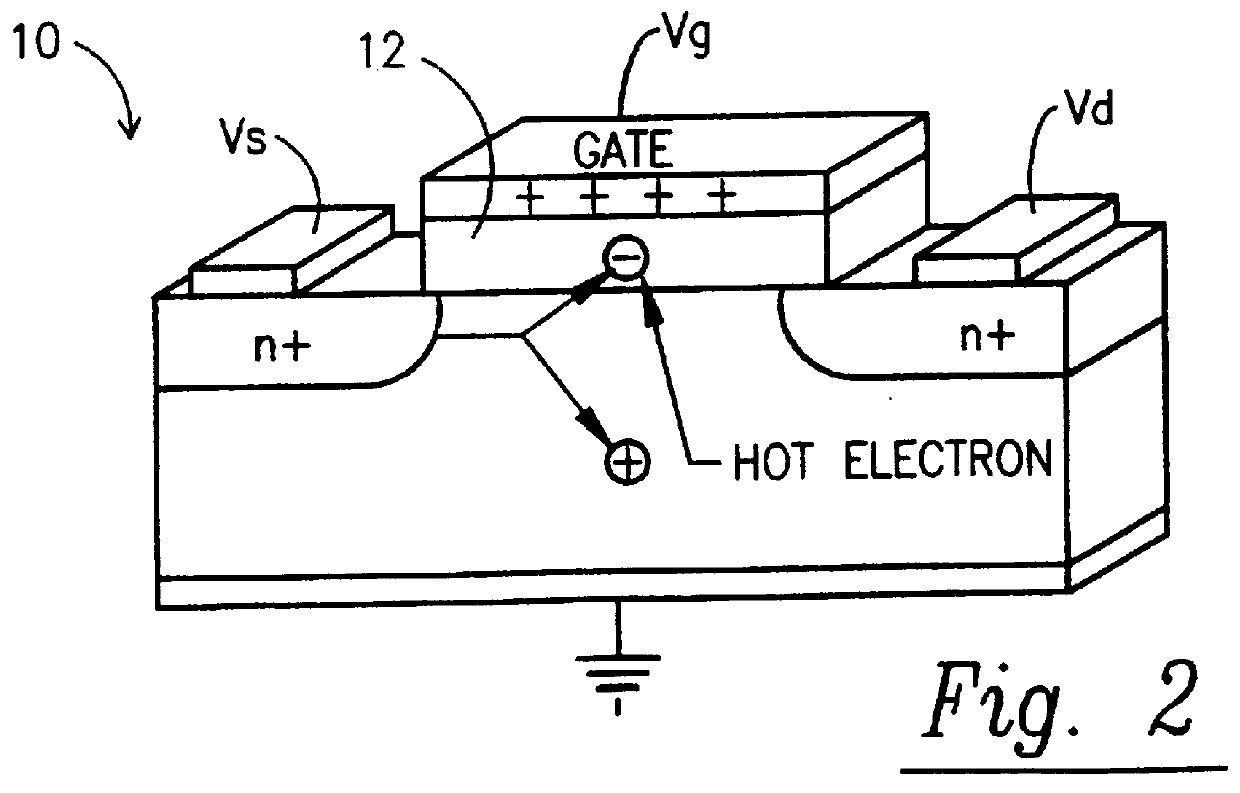
Some reliability concerns in deep submicron ICs are caused by short channel effects which are far more damaging in scaled devices than in near-micron devices.
Despite the success of applying conventional scaling rules to devices scaled from 2 .mu.m to 1 .mu.m, the same rules do not apply when devices are further scaled down to deep submicron features.
Although IDDQ testing is used successfully with near-micron CMOS processes, its feasibility in deep submicron (L.sub.effective <0.5 .mu.m) CMOS processes has not been
fully developed.
In expanding the utilization of IDDQ testing into the deep submicron regime, many problems exist with the current techniques and circuit designs presently being used in the industry.
IDDQ testing imposes several penalties on
present day CMOS ICs including
circuit under test (
CUT) performance degradation, increased IC area overhead, and low test speed versus current resolution sensing ratio.
However, as IC feature sizes are scaled down to deep submicron levels, the penalties associated with IDDQ testing increase significantly.
These additional faults are due to strong device interdependencies and specification tolerances resulting from scaled features.
Thus, the problems associated with the IDDQ testing techniques and circuit designs currently being used in the industry in contemporary CMOS technologies severely limit the use of IDDQ testing in deep submicron applications.
The external testing approach presents several problems which renders its use in deep submicron applications impractical.
It is therefore impractical to employ a
linear element such as a
resistor to both sink and detect the current since both conditions cannot be met simultaneously.
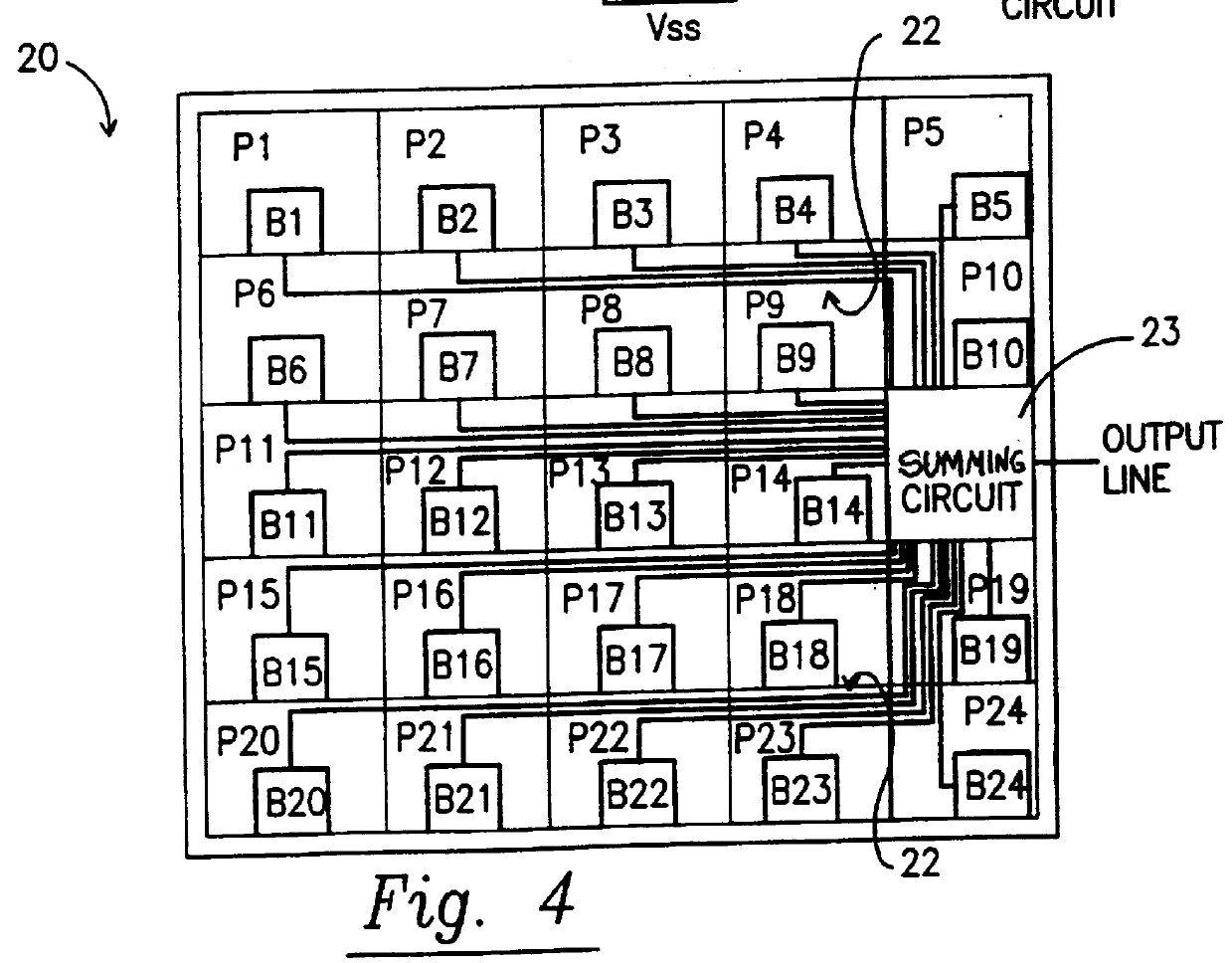
While all of the above referenced examples of internal built in current sensor circuits have been used in near-micron ICs, none of them are suitable for use in deep submicron applications due to their lack of current sensitivity, excessive area overhead, required additional amplifiers and summing circuits, excessive
circuit complexity and larger operating power requirements.
This minimum
voltage limits the sensitivity and ultimate
current range of the detecting portion of the circuit.

