Debug interface including timing synchronization logic

a timing synchronization logic and interface technology, applied in the field of computer systems, can solve the problems of increasing the burden on application software developers, the cost of developing and debugging new software products, and the complexity of softwar

Inactive Publication Date: 2000-11-07
ADVANCED MICRO DEVICES INC
View PDF49 Cites 68 Cited by
  • Summary
  • Abstract
  • Description
  • Claims
  • Application Information

AI Technical Summary

Problems solved by technology

The growth in software complexity, in combination with increasing processor clock speeds, has placed an increasing burden on application software developers.
The cost of developing and debugging new software products is now a significant factor in processor selection.
A failure to include adequate software debug functionality in a processor results in longer customer development times and reduces attractiveness of the processor for use within industry.
However, the initial task of getting the operating systems running reliably often calls for special development equipment.
The custom design of emulator interfaces in increasingly unrealistic and expensive as product life cycles are reduced and nonstandard and exotic integrated circuit packages are predominant in present day processor design.
Few known processor manufacturing techniques are available that include a suitable full-function in-circuit emulation functionality.
Multiplexing of pins is not desirable in embedded controllers, which inherently suffer from overload of pin functionality.
However in debug environments with high branch activity and low cache hit rates, BTA-cycles are often fully occupied handling branches, resulting in a conflict over access to the address bus that necessitates processor "throttle back" to prevent a loss of instruction trace information.
For example, software in the communications industry is branch-intensive and suffers poor cache utilization often resulting in 20% or more throttle back, an unacceptable amount for embedded products which are subject to real-time constraints.
The bond-out approach suffers from the need to support additional bond pad sites in all fabricated devices, a burden in small packages and pad limited designs, particularly if a substantial number of extra pins are required by the debug support variant.
Furthermore, the debug capability of specially packaged processors is unavailable in typical processor-based production systems.
The BDM system includes trace support, but not conveniently using the serial link.
Instead the BDM system supplies trace support through additional dedicated pins and expensive external trace capture hardware that transfer instruction trace data.
Accordingly, present day techniques for software debugging suffer from a variety of limitations including increased packaging and development costs, circuit complexity, processor throttling, and bandwidth matching difficulties.
Furthermore, no adequate low-cost procedure for providing trace information is currently available.
The limitations of the existing solutions are likely to be exacerbated in the future as internal processor clock frequencies continue to increase.

Method used


Image

  • Debug interface including timing synchronization logic
  • Debug interface including timing synchronization logic
  • Debug interface including timing synchronization logic

Examples


Embodiment Construction

)

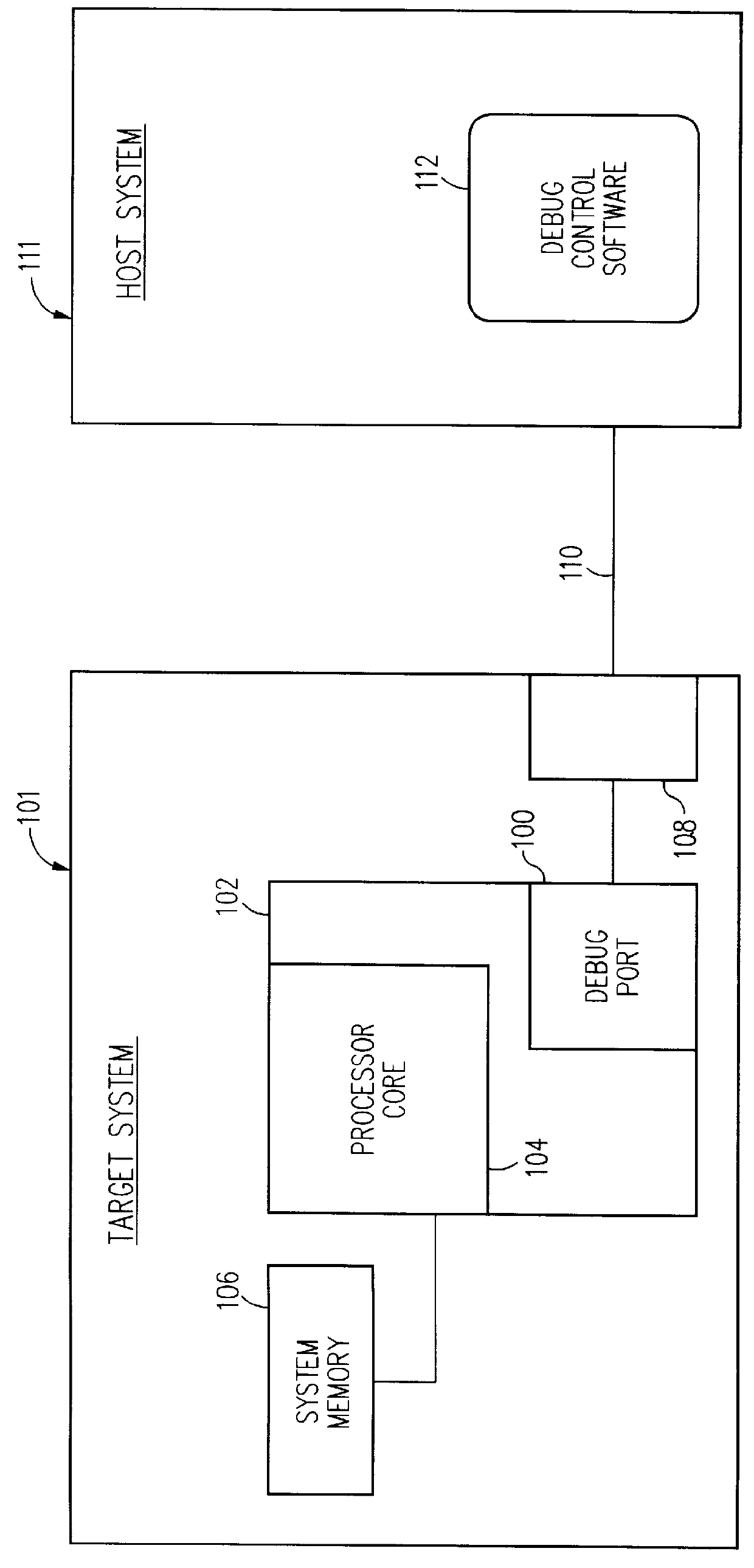
Referring to FIG. 1, a schematic block diagram illustrates a software debug environment utilizing a debug port 100. A target system 101 is shown containing an embedded processor device 102 coupled to system memory 106. The embedded processor device 102 is an integrated debug interface for flexible, high-performance in an embedded hardware / software debug system. The embedded processor device 102 includes a processor core 104 and the debug port 100. In some embodiments, the embedded processor device 102 may incorporate additional circuitry (not shown) for performing application specific functions, or may take the form of a stand-alone processor or digital signal processor. In the illustrative embodiment, the debug port 100 includes an IEEE-1149.1-1990 compliant JTAG interface or other similar standardized serial port interface.

A host system 111 is used to execute debug control software 112 for transferring high-level commands and controlling the extraction and analysis of debug infor...


PUM


Abstract

A system for debugging a processor includes a logic circuit for communicating commands and data between an input/output port which operates at a first clock frequency, and trace control logic which operates at a second clock frequency that is different from the first clock frequency. In some embodiments, the input/output port is a JTAG (Joint Test Action Group) port operating at a maximum clock frequency of 25 MHz and the trace control logic operates at a clock frequency of 33 Mhz, 66 MHz, 99 MHz, or 133 mhz. A suitable JTAG clock frequency is a minimum of either half the CPU internal clock frequency or 2.25 Mhz for synchronizing the internal signals between different clock frequencies. When the input/output port, which is typically a serial/parallel input/output port, writes data to debug registers, including ITCR, DCSR, soft-address, and RX-DATA registers, timing strobe signals to the registers are synchronized to a processor clock to reduce the synchronization logic for register bits that are used by the processor and trace control logic. By synchronizing the debug register data write operations to the processor clock timing, the data bits of the registers are used by the processor and the trace logic without further synchronization. Advantageously, the amount of synchronization logic is reduced. Synchronizing the signals that cross the blocks with different clock timing facilitates communication between the processor, the trace control logic, and the serial and parallel input/output ports and reduces the amount of synchronization logic.

Description

1. Field of the InventionThe present invention relates to computer systems such as microprocessors. More specifically, the present invention relates to a software debug support system and operating method in processors.2. Description of the Related ArtThe growth in software complexity, in combination with increasing processor clock speeds, has placed an increasing burden on application software developers. The cost of developing and debugging new software products is now a significant factor in processor selection. A failure to include adequate software debug functionality in a processor results in longer customer development times and reduces attractiveness of the processor for use within industry. Software debug support is particularly useful in the embedded products industry, where specialized on-chip circuitry is often combined with a processor core.The software debug tool configuration of a processor addresses the needs of several parties in addition to the software engineer wh...

Claims


Application Information

Patent Timeline
Patent Type & Authority Patents(United States)
IPC IPC(8): G06F11/36G06F11/34
CPCG06F11/3632G06F11/3656G06F11/3636G06F11/3466
Inventor MADDURI, VENKATESWARA RAO
Owner ADVANCED MICRO DEVICES INC
Why Eureka
Try Eureka