Two step oxide removal for memory cells

a memory cell and oxide removal technology, applied in the direction of electrical equipment, semiconductor devices, capacitors, etc., can solve the problems of large linewidth devices, large particle sizes, and particle generation, and achieve the effect of minimizing defective memory cells and reducing particles

Inactive Publication Date: 2001-01-16
TEXAS INSTR INC
View PDF24 Cites 25 Cited by
  • Summary
  • Abstract
  • Description
  • Claims
  • Application Information

AI Technical Summary

Benefits of technology

A two step insitu oxide strip significantly reduces particles and minimizes defective memory cells. Following an inital exposure to vapor HF for oxide removal, a first insitu water rinse occurs. A second exposure to vapor HF then occurs and is followed by a second insitu water rinse. During both the first water rinse and the second water rinse, the wafer may be rotated at increasing speeds which aids in sweeping particles off the wafer surface. Water, rather than water vapor, aids in freeing particles from the wafer surface which may contain complex topographies. The process may be practiced in a commercially available reactor, such as one manufactured by FSI, and is particularly suitable for ULSI devices such as 64 megabit DRAMs employing crown type memory cells.

Problems solved by technology

A problem with wet etching silicon dioxide and subsequent tank rinsing is particle generation.
However, as linewidths continue to shrink, small particles that may not have affected larger linewidth devices, become more problematical as they do affect smaller linewidth devices.
Particle control is a problem regardless of the type of memory cell architecture used for the DRAM.
However, such technique could possibly generate thousands of particles which could settle back onto the wafer surface.
However, even the advantageous techniques described in the patent may not be enough to successfully minimize particle disruption for ULSI devices such as DRAMS having complex topographies.

Method used


Image

  • Two step oxide removal for memory cells
  • Two step oxide removal for memory cells
  • Two step oxide removal for memory cells

Examples


Embodiment Construction

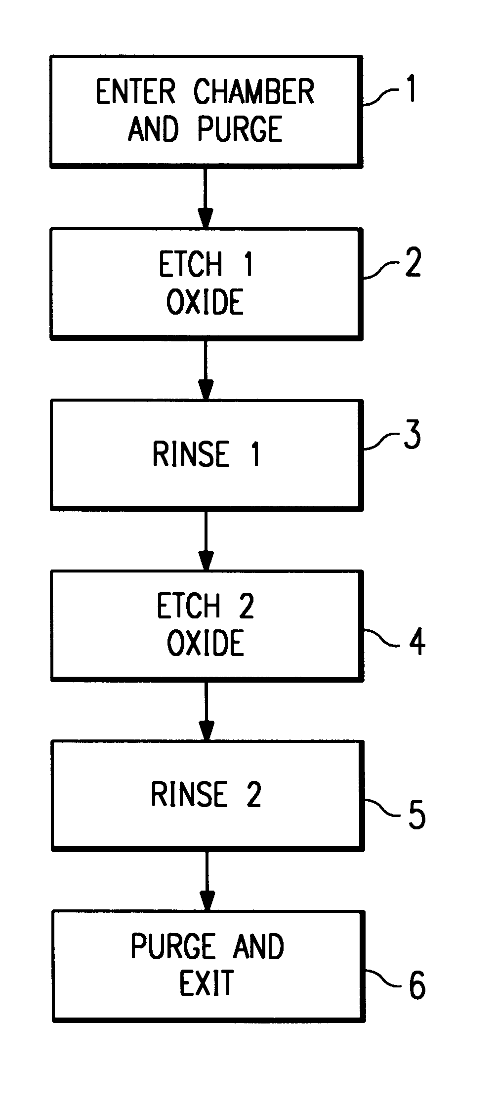
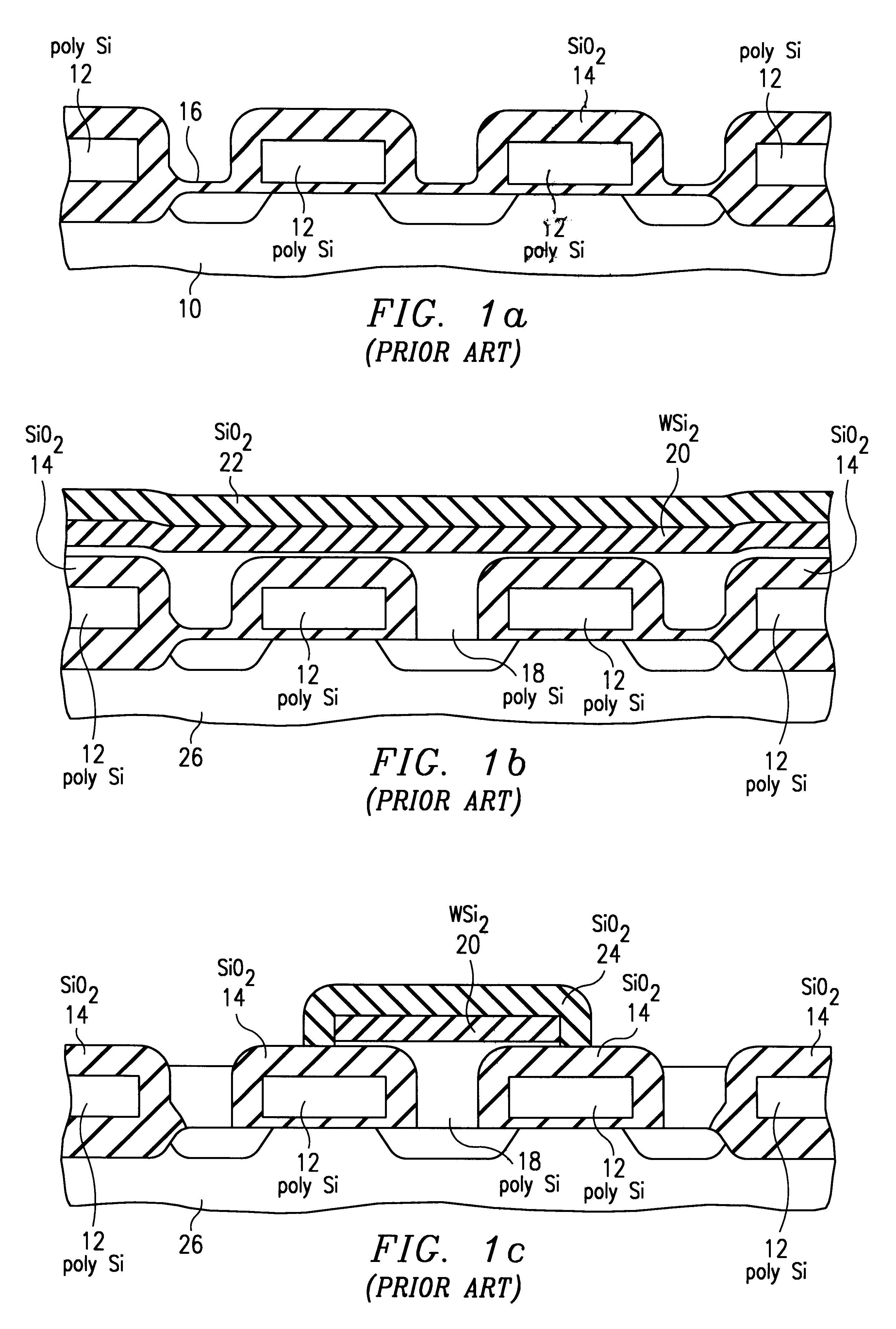
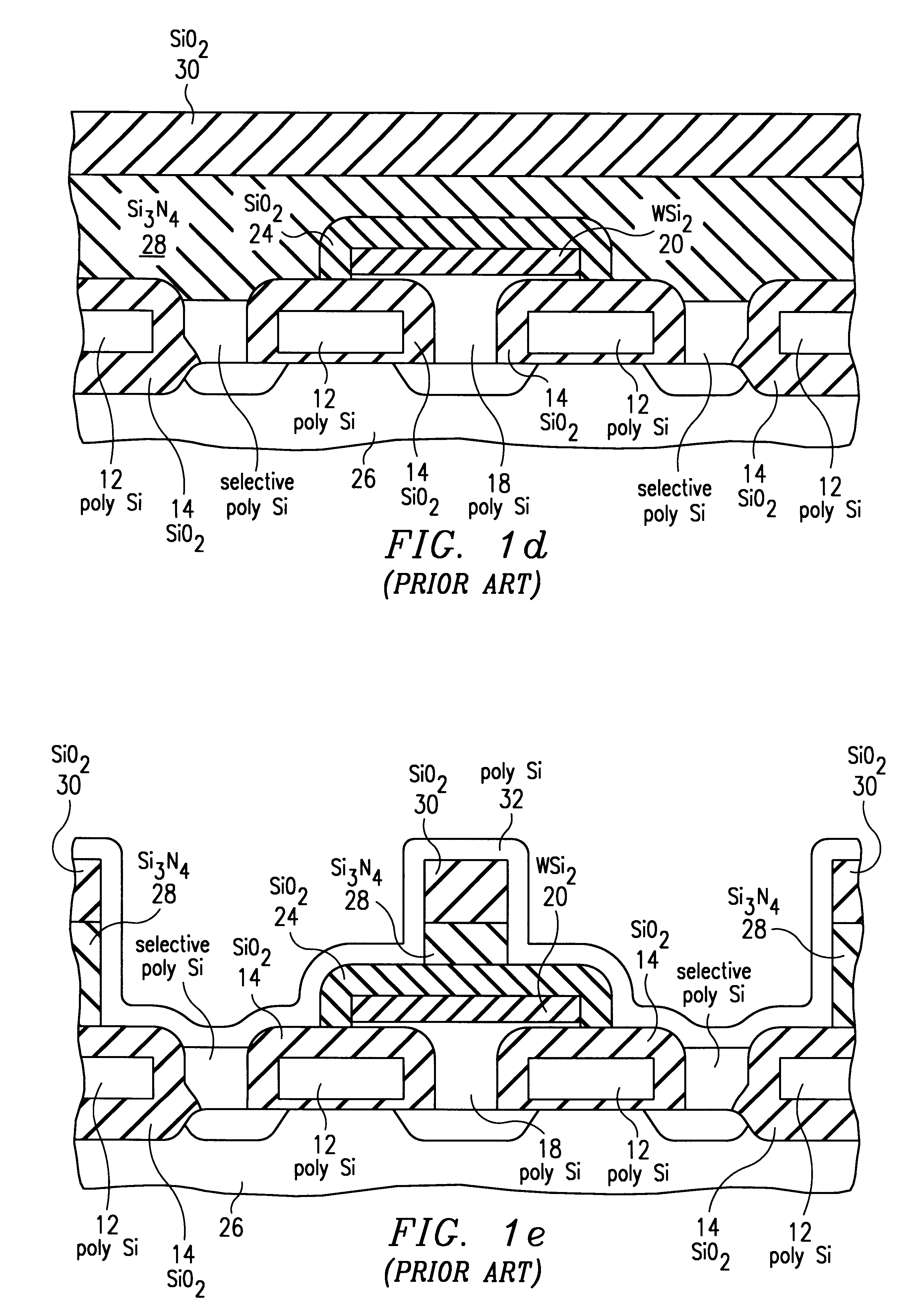
FIG. 2 depicts, in flow chart form, a two step oxide cleaning process according to the preferred embodiment of the invention. Relating FIG. 2 to prior art FIGS. 1a-1f, the inventive two step oxide cleaning process would be used to remove the oxide layer 30 during the steps shown between FIGS. 1e and 1f during crown cell formation. Of course, crown type memory cells may be made by other processes, some of which are described in the aforementioned U.S. patents. Regardless of the specific process used to manufacture the crown memory cell, each process will implement an oxide strip and thus the inventive two step oxide cleaning process is suitable for all crown memory cell processes. Additionally, the inventive two step oxide strip is not limited to crown memory cells and is applicable to other types of memory cells and to semiconductor processing in general as oxides are widely used.

In the following description, it is to be noted that the ratios between nitrogen, water vapor and HF hav...


PUM


Abstract

Hydrofluoric acid (HF) mixed with water and often buffered with ammonium fluoride is a standard silicon dioxide wet etchant which is followed by a rinse. An improved silicon dioxide etch is vapor HF which may be followed by a water vapor rinse. The invention discloses a further improved silicon dioxide etch. Following an initial exposure to vapor HF for oxide removal, a first insitu water rinse occurs. A second exposure to vapor HF then occurs and is followed by a second insitu water rinse. Water, rather than water vapor, aids in freeing particles from the wafer surface. During both the water rinses, the wafer may be rotated at increasing speeds to aid in sweeping particles from wafer surface. The process may be practiced in a commercially available reactor and is suitable for ULSI devices having complex topographies, such as, for example, 64 megabit DRAMs employing crown type memory cells.

Description

The invention relates generally to the field of semiconductor processing and more specifically to removing oxide from semiconductor wafers.BACKGROUND OF INVENTIONSilicon dioxide, SiO.sub.2, is commonly used as a dielectric material in semiconductor manufacturing. The dielectric may be formed by various methods, such as by plasma deposition, TEOS decomposition and thermal growth. Regardless of the manner of oxide formation, it is necessary to remove or pattern the oxide. One way to pattern oxide is by plasma etching, also known as dry etching, as described in Plasma Etching, by Manos and Flamm, copyright 1989, pages 159-165. Another way to pattern oxide is by wet etching as described in Semiconductor Integrated Circuit Processing Technology, by Runyan and Bean, copyright 1990, pages 264-266. Hydrofluoric acid (HF) mixed with water and often buffered with ammonium fluoride is a standard silicon dioxide wet etchant. Typically, the semiconductor wafer is immersed into a tank containing ...

Claims


Application Information

Patent Timeline
Patent Type & Authority Patents(United States)
IPC IPC(8): H01L21/02H01L21/306H01L21/311H01L21/316H01L27/108
CPCH01L21/02054H01L21/31116H01L28/40H01L21/31637H01L27/10814H10B12/315H01L21/02183
Inventor DOSHI, VIKRAM N.TOMOMATSU, HIROCLARK, ROY D.GULDI, RICHARD L.
Owner TEXAS INSTR INC
Why Eureka
Try Eureka