

Low thermal expansion circuit board and multilayer wiring circuit board
- Summary
- Abstract
- Description
- Claims
- Application Information
AI Technical Summary
Benefits of technology
Problems solved by technology
Method used
Image

Examples
example 1
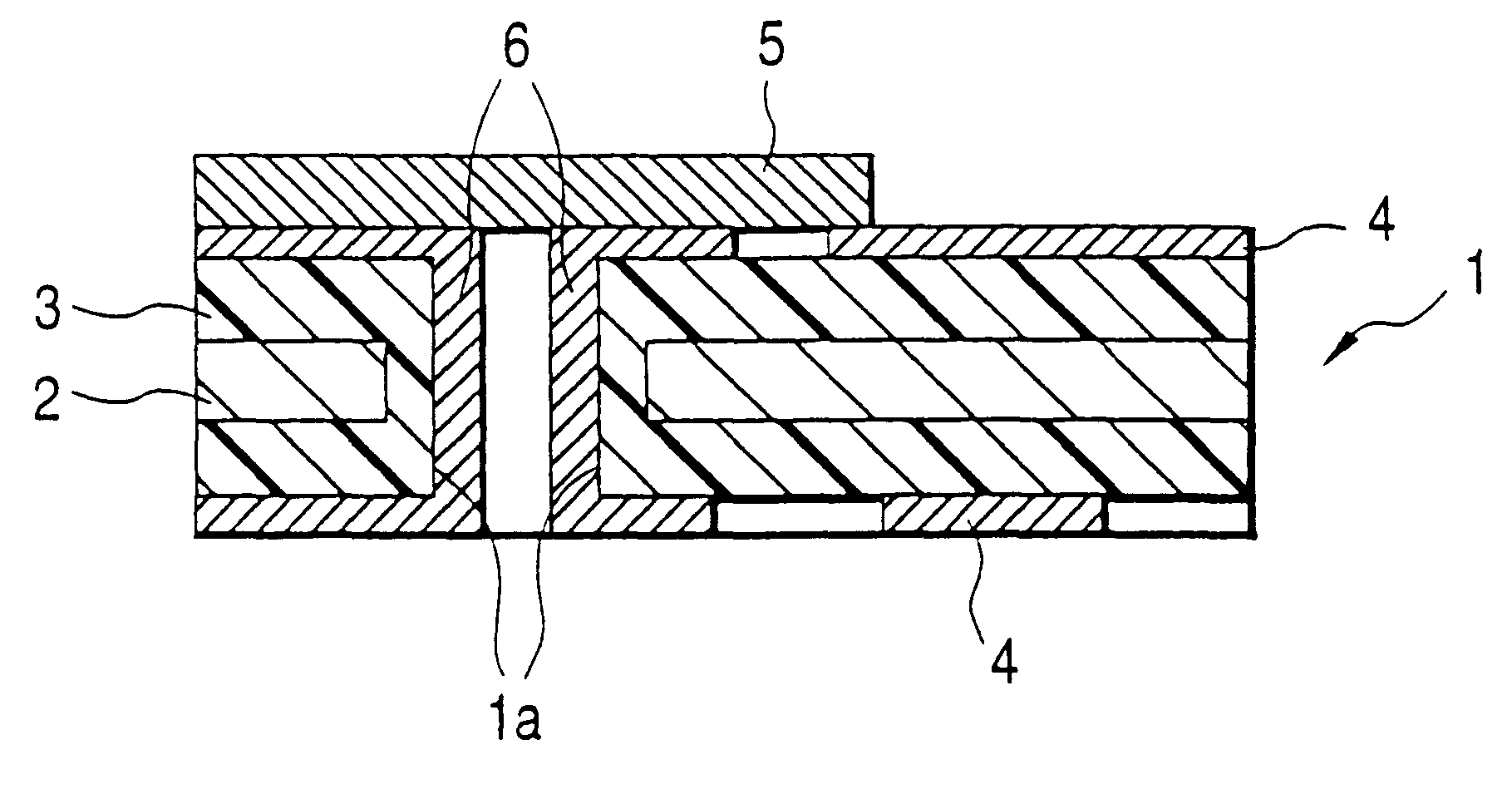
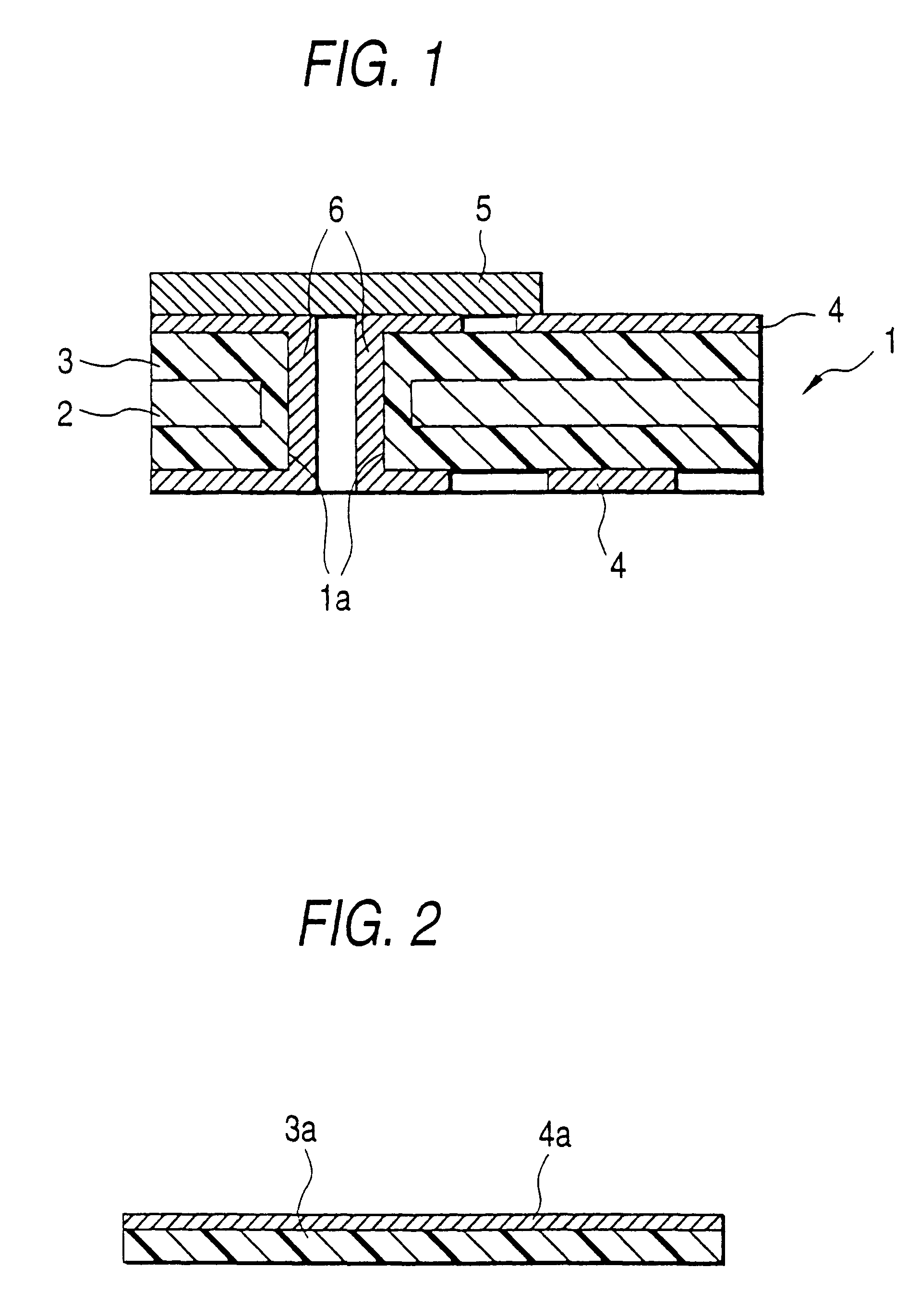
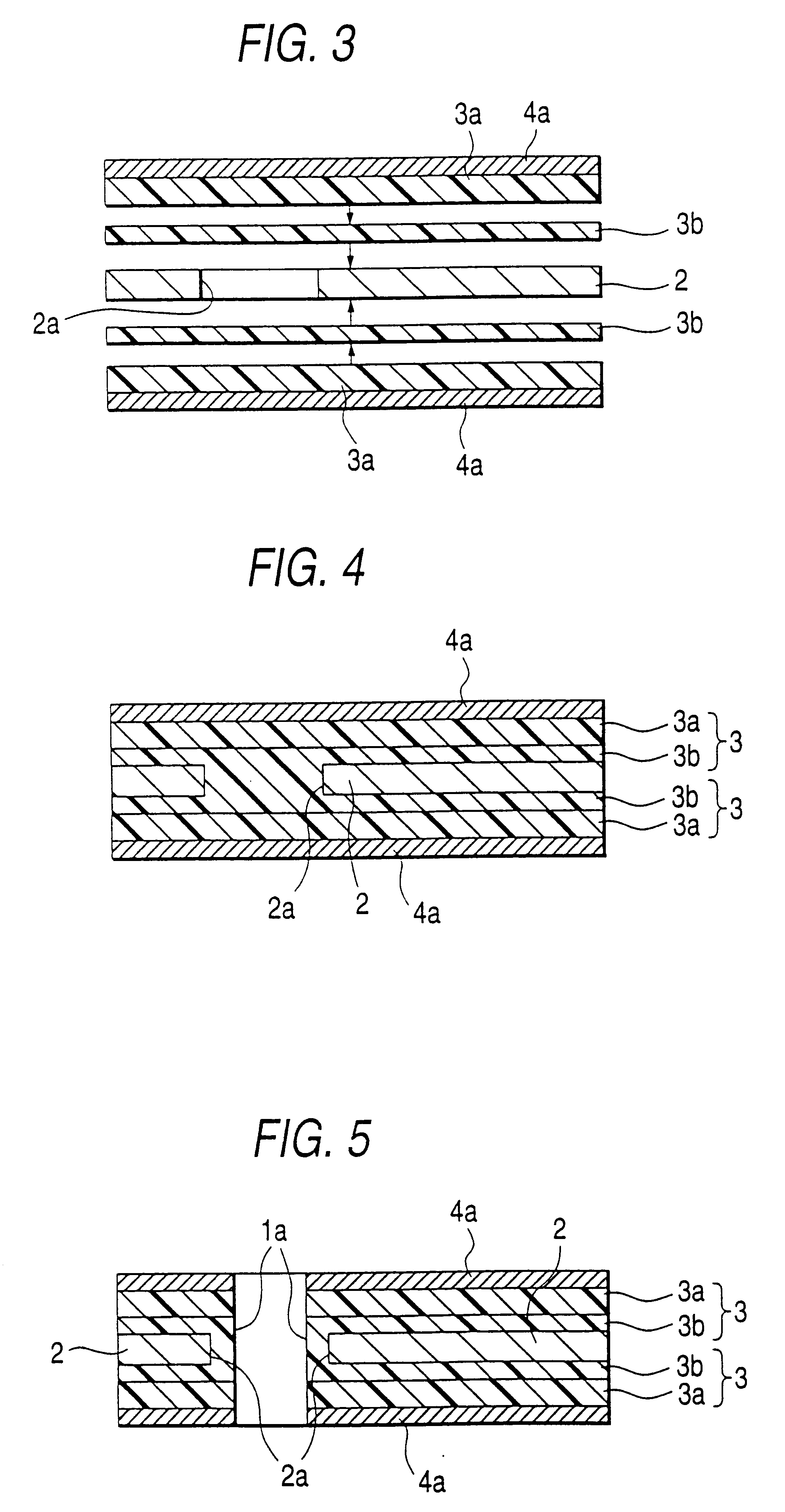
A polyimide precursor varnish (a polyamic acid varnish obtained by reacting p-phenylenediamine and 3,3',4,4'-biphenyltetracarboxylic acid dianhydride in N-methylpyrrolidone) was applied to a 18 .mu.m thick copper foil 4a, dried, and heated at 400.degree. C. in a nitrogen atmosphere for 1 hour to form a polyimide layer 3a having a thickness of 20 .mu.m (see FIG. 2).
A 50 .mu.m thick 42 alloy foil 2 (Ni: 42%; Fe: 58%; thermal expansion coefficient: 4.5 ppm / .degree. C.) having holes 2a made with a drill of 0.3 mm in diameter at prescribed positions was prepared, and the copper / polyimide laminate above prepared was bonded to each side of the foil 2, with its copper foil outside, via a polyimide adhesive sheet 3b (SPB-035A, produced by Nippon Steel Chemical Co., Ltd.) by hot-pressing at 200.degree. C. under a pressure of 40 kg / cm.sup.2 for 1 hour (see FIG. 3) to obtain a low-expansion double sided board, in which the polyimide layer 3a and the polyimide adhesive sheet 3b formed an insulat...
example 2
A low thermal expansion circuit board 1A (with no adhesive resin layer 5) was prepared in the same manner as in Example 1. Holes 9a were made through an adhesive sheet 9 (SPB-035A, produced by Nippon Steel Chemical Co., Ltd.) with a drill (diameter: 0.2 mm) at positions corresponding to the electrodes 11 of the circuit board 1 (see FIG. 11). The adhesive sheet 9 was bonded at 180.degree. C. under a pressure of 30 kg / cm.sup.2 for 30 minutes onto a right position of the circuit board 1A. The holes 9a of the adhesive sheet 9 were filled with soldering paste (Sn820RA-3AMQ, produced by Nippon Superior K.K.; melting point: 240.degree. C.) by screen printing, and the soldering paste was fused at 270.degree. C. to form soldering bumps 10 (see FIG. 9). Two low thermal expansion circuit boards 1A each having soldering bumps 10 and a low thermal expansion circuit board 1A having neither the adhesive sheet 9 nor the soldering bump 10 as a top circuit board were laminated at prescribed positions...
example 3
A low-expansion circuit board 1A (.alpha.: 7.5 ppm / .degree. C.) was prepared in the same manner as in Example 1. The same polycarbodiimide solution as used in Example 1 was applied on the entire surface of the mount side of the circuit board 1A to a dry thickness of 80 .mu.m and dried to form an adhesive resin layer 5. A silicon chip was mounted thereon in the same manner as in Example 1.
PUM
| Property | Measurement | Unit |
|---|---|---|
| Percent by mass | aaaaa | aaaaa |
| Thickness | aaaaa | aaaaa |
| Thermoplasticity | aaaaa | aaaaa |
Abstract
Description
Claims
Application Information