

Semiconductor device
a technology of semiconductors and transistors, applied in semiconductor devices, radio frequency controlled devices, electrical equipment, etc., can solve the problems of reducing the mobility of the mosfet, limiting the field effect mobility, etc., and reducing the mobility
- Summary
- Abstract
- Description
- Claims
- Application Information
AI Technical Summary
Problems solved by technology
Method used
Image

Examples
first embodiment
[First Embodiment]
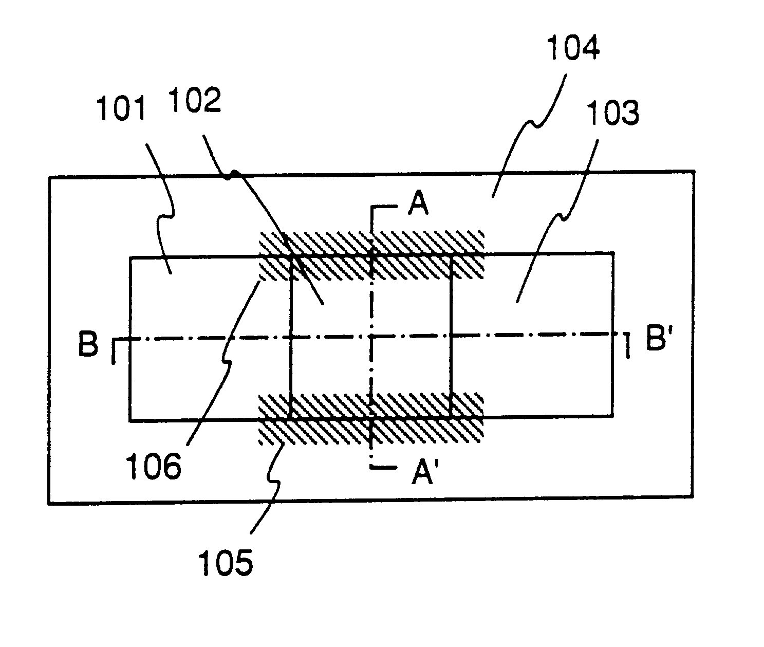
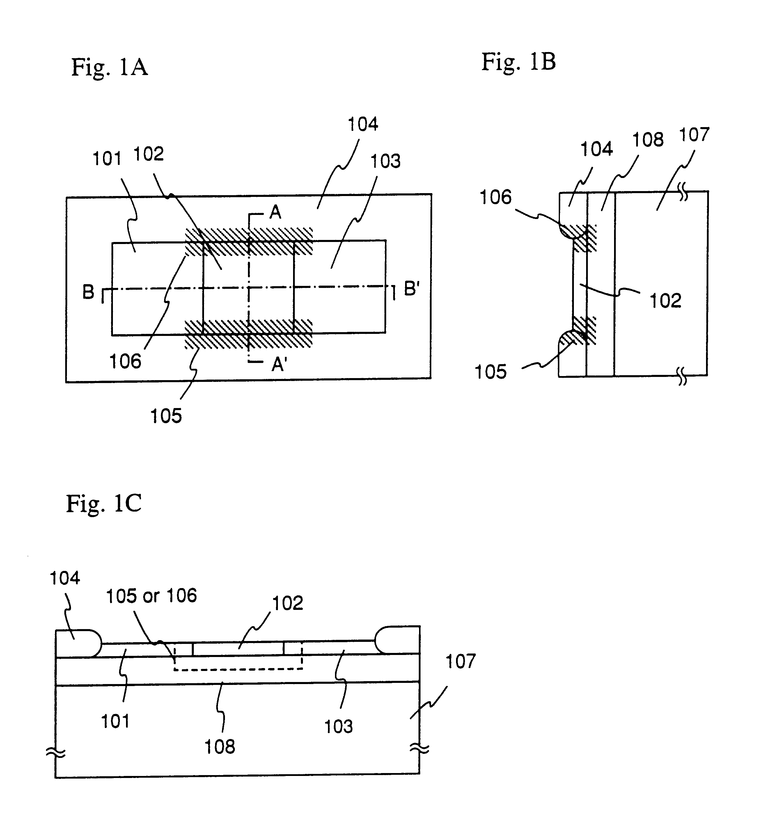
At first, a structure of an active region (hereinafter a source region, a channel forming region and a drain region will be called collectively as such) of an N-channel type pinning FET of the present invention will be explained with reference to FIGS. 1A through 1C.
It is noted that a case of using an SOI substrate called an SIMOX substrate as a substrate for fabricating the pinning FET will be illustrated in the present embodiment. The SIMOX substrate is what a buried oxide film is formed by implanting oxygen into a mono-crystal silicon substrate and a mono-crystal silicon layer left on the buried oxide film is utilized as an active region.
FIG. 1A is a plan view of the active region of the N-channel type pinning FET, FIG. 1B is a scion view taken along a line A-A' in the plan view of FIG. 1A and FIG. 1C is a section view taken along a line B-B' in the plan view of FIG. 1A.
As shown in FIG. 1A, the active region of the N-channel type pinning FET comprises a source r...
second embodiment
[Second Embodiment]
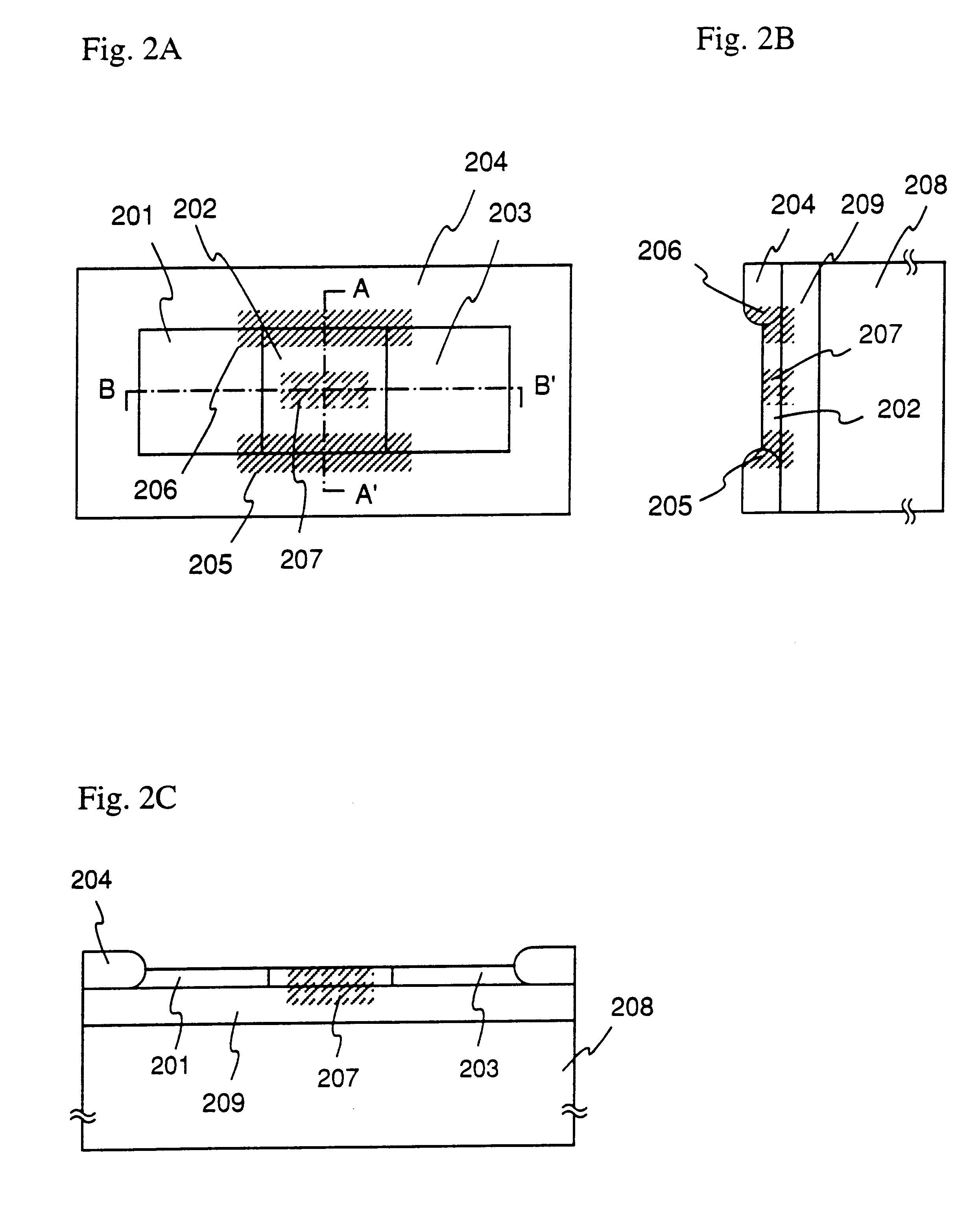
A structure of an active region of a P-channel type pinning FET of the invention will be explained in the present embodiment with reference to FIGS. 2A through 2C. It is noted that the case of using the SIMOX substrate similarly to the first embodiment will be shown in the present embodiment.
Similarly to FIGS. 1A through 1C used in the first embodiment, FIG. 2A is a plan view of the active region of the P-channel type pinning FET, FIG. 2B is a section view taken along a line A-A' in the plan view of FIG. 2A and FIG. 2C is a section view taken along a line B-B' in the plan view of FIG. 2A. It is noted that description of a gate insulating film, a gate electrode, an interlayer insulating film, a fetch electrode and the like is omitted and only the active region will be explained in the present embodiment similarly to the first embodiment.
However, because the basic structure of the N-channel type pinning FET and the P-channel type pinning FET is same, the pinning eff...
third embodiment
[Third Embodiment]
The case of forming the pinning FET on the mono-crystal silicon substrate has been explained in the first and second embodiments. In such cases, the active region (the source region, channel forming region and drain region) is made from the weak N or P-type mono-crystal silicon.
However, the semiconductor which can be utilized in the present invention is not limited to the mono-crystal silicon. That is, it is possible to form the active region or at least a part thereof by a compound semiconductor or by a laminating the compound semiconductor and the mono-crystal silicon.
For instance, gallium arcenide (GaAs), indium phosphide (InP) or silicon germanium (Si.sub.x Ge.sub.1-x : where x is 0.5 to 9.5) may be used as the compound semiconductor.
When the compound semiconductor of Si.sub.x Ge.sub.1-x is used for the channel forming region in particular, a carrier mobility higher than the case of using mono-crystal silicon can be obtained. That is, it is possible to realize ...
PUM
 Abstract
Description
Claims
Application Information