Wide wavelength range high efficiency avalanche light detector with negative feedback

a technology of avalanche light and negative local feedback, which is applied in the field of light detection, can solve the problems of limiting the ability to detect light, limiting the use of multi-channel elements with high gain, and difficult production of large area and multi-channel elements with high gain, and achieves the effect of low impedance substra

Inactive Publication Date: 2001-04-24
BOARD OF RGT THE UNIV OF TEXAS SYST
View PDF7 Cites 24 Cited by
  • Summary
  • Abstract
  • Description
  • Claims
  • Application Information

AI Technical Summary

Problems solved by technology

However, semiconductors may also have unbound electrons that form a "sea" of electrons that can move around freely in the material.
The p-i-n structure can present such disadvantages as high working bias (hundreds of Volts), need for cooling systems, and difficulty in the production of large area and multi-channel elements with high gain, which strongly limits their use to a relatively small number of applications.
Although initial results of conventional CRS detector tests are encouraging, especially since they have good spectral efficiency for the long wave range of light spectrum, there are some shortcomings in the CRS design that limit their abilities to detect light.
Another drawback is the requirement for the resistive layer to be transparent for the blue light, while having an electrical resistance high enough to quench avalanche multiplication.
In addition, present CRS detectors have a diffusion zone behind the sensitive depleted region which can decrease time resolution and increase noise resulting from delayed charge carriers.
Another disadvantage of CRS detectors is that a significant amount of the diode area is passive.
The passivity which results from the circular geometry of the heavily doped n regions can hinder the enhancement of the electric field necessary for avalanche multiplication.

Method used


Image

  • Wide wavelength range high efficiency avalanche light detector with negative feedback
  • Wide wavelength range high efficiency avalanche light detector with negative feedback
  • Wide wavelength range high efficiency avalanche light detector with negative feedback

Examples


Embodiment Construction

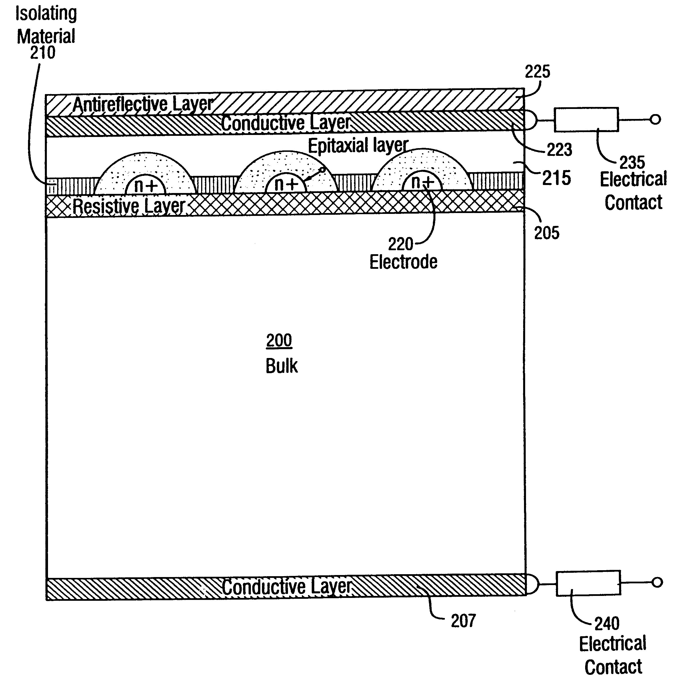
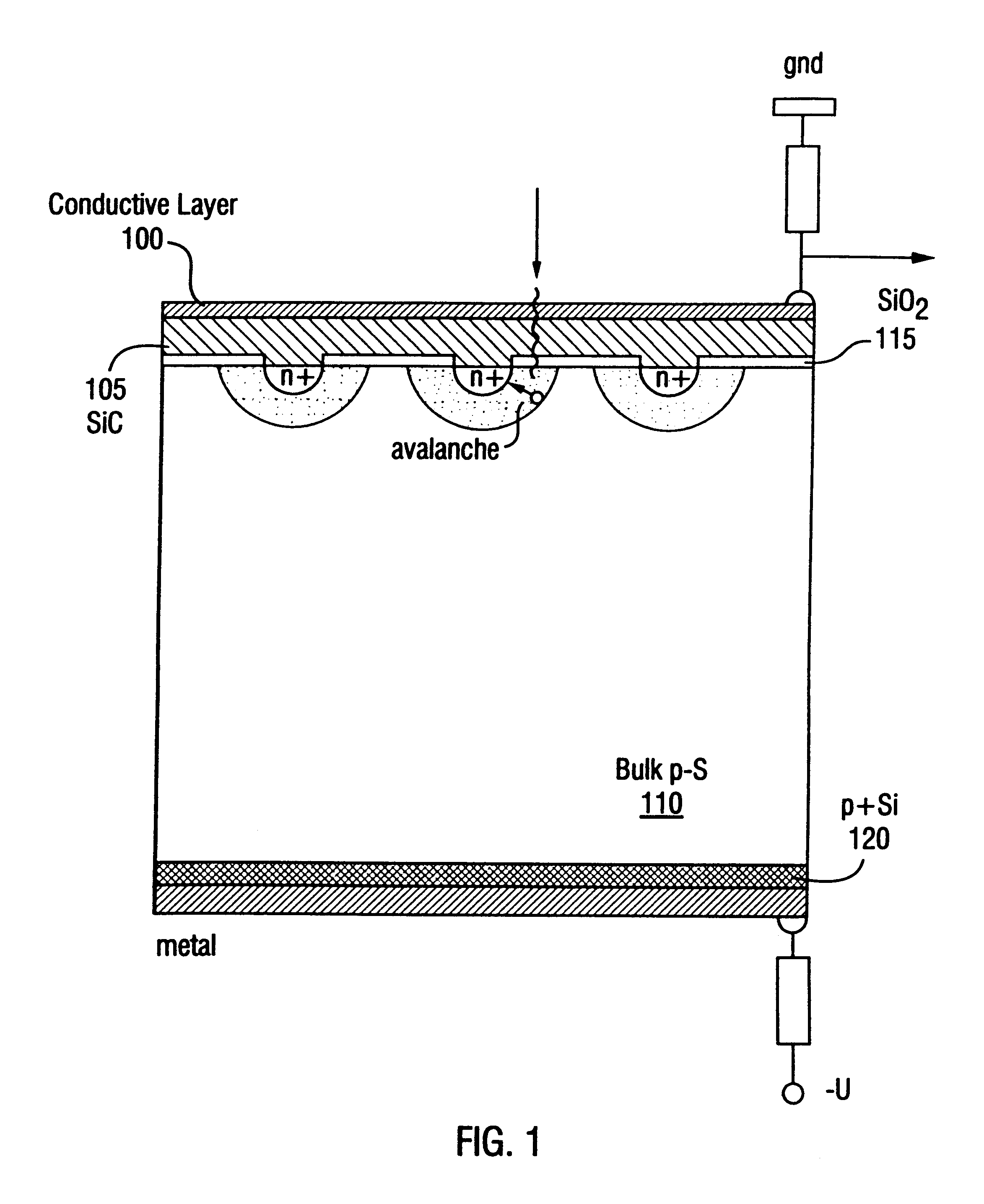
Illustrative embodiments of the invention are described below as it might be employed in a novel design of a conductor-resistor-semiconductor (CRS) avalanche detector for photon detection and signal amplification. In the interest of conciseness, not all features of an actual implementation are described in this specification. It will of course be appreciated that in the development of any such actual embodiment numerous implementation-specific decisions must be made to achieve the developers' specific goals, such as compliance with system-related and business-related constraints, which will vary from one implementation to another. Moreover, it will be appreciated that though such a development effort might be complex and time-consuming, it would nevertheless be a routine undertaking for those of ordinary skill having the benefit of this disclosure.

5.1 Overview

When light quantum enters a substrate (e.g., silicon), it creates an electron-hole pair. The electrons are collected in a sma...


PUM


Abstract

A novel use of a solid state light detector with a low impedance substrate is described. Light that enters the substrate after traversing the antireflective layer creates an electron-hole pair. The electrons are collected in a crystalline epitaxial layer that spans the space charge region, or depletion layer. A high electric field accelerates free electrons inside the depletion region. The electrons collide with the lattice to free more holes and electrons resulting from the presence of an n-p junction, or diode. The diode is formed by placing the crystalline layer which has positive doping in close proximity with the electrodes which have negative doping. The continual generation of charge carriers results in avalanche multiplication with a large multiplication coefficient. During the avalanche process, electrons can be collected enabling light detection. A resistive layer is used to quench, or stop, the avalanche process.

Description

1. FIELD OF THE INVENTIONThe invention relates in general to the field of light detection using semiconductor devices, and more particularly, to the use of exceptionally designed avalanche diodes for light detection. Specifically, the invention relates to a novel design of conductor-resistor-semiconductor (CRS) avalanche detector with negative local feedback for photon detection and signal amplification.2. BACKGROUND OF THE INVENTIONIn semiconductor material, light with a wavelength between 300 nm and 1100 nm attenuates generating charge carriers (i.e., holes and electrons). In an intrinsic material, the small concentration of holes equals the concentration of electrons. In contrast, a doped material has a higher concentration of one charge carrier (e.g., more electrons than holes). A doped material that has more electrons is called n-type, while a doped material that has more holes is called p-type. Heavily doped materials, indicated by the addition of a plus sign after the n or p ...

Claims


Application Information

Patent Timeline
Patent Type & Authority Patents(United States)
IPC IPC(8): H01L31/102H01L31/115H01L31/107
CPCH01L31/107H01L31/115
Inventor ANTICH, PETER P.TSYGANOV, EDWARD N.
Owner BOARD OF RGT THE UNIV OF TEXAS SYST
Why Eureka
Try Eureka