Method for etching multilayer compound semiconductor material

a semiconductor material and compound technology, applied in the direction of individual semiconductor device testing, semiconductor/solid-state device testing/measurement, instruments, etc., can solve the problem of increasing the generation of defects

Inactive Publication Date: 2001-10-23
ZORY JR PETER S
View PDF1 Cites 6 Cited by
  • Summary
  • Abstract
  • Description
  • Claims
  • Application Information

AI Technical Summary

Benefits of technology

When the pulse anodization occurs in a solution which etches the oxide, a "traveling oxide" effect occurs. After a time, the current pulse attains a steady state shape, and the oxide "sinks into" the surface of the semiconductor. The oxide thickness remains constant in time, the oxide dissolves at the same average rate as it forms, and the semiconductor material is removed as sketched in FIG. 6 where a trench 22 is formed in the cladding layer 6 extending through the active layer 4 to the lower cladding layer 7. The native oxide 24 is left on the sides and bottom of the trench 22. At the end of the process, a ridge of ridge height h.sub.r 23 is left under the protecting photoresist 8. The oxide etch rate has been measured to be 16 nm / min for Al.sub.0.6 Ga.sub.0.4 As native oxide formed by the method of the present invention.

Problems solved by technology

This step generally requires heating the wafer which can increase the defects generated by heating and cooling the many layers of different material.

Method used


Image

  • Method for etching multilayer compound semiconductor material
  • Method for etching multilayer compound semiconductor material
  • Method for etching multilayer compound semiconductor material

Examples


example 2

AlGaInAs Laser Diode Laser Bars

A laser wafer with a AlGaInAs quantum well, denoted L362, which is sketched in FIG. 10, was divided in two. One half the wafer was processed into gain guided laser diode bars by the method of the present invention as shown in FIGS. 6a-c, the other half was processed into bars of 100 micron wide by 500 micron long lasers by a prior art process of depositing SiO.sub.2, opening 100 micron wide slots in the SiO.sub.2, and metalization. Ridge heights of 200 nm and oxide thicknesses of 100 nm were used. The threshold currents I.sub.th and differential quantum efficiencies (DQE) are given in Table 3.

example 3

AlGInAs Laser Diodes

A laser wafer with a AlGaInAs quantum well, denoted E1795, which is sketched in FIG. 11, was divided in two. One half the wafer was processed into gain guided laser diode bars by the method of the present invention as shown in FIGS. 6a-c, the other half was processed into bars of 100 micron wide by 500 micron long lasers by a prior art process of depositing SiO.sub.2, opening

100 micron wide slots in the SiO.sub.2, and metalization. Ridge heights of 200 nm and oxide thicknesses of 100 nm were used. The threshold currents I.sub.th and differential quantum efficiencies (DQE) are given in Table 4.

example 4

(AlGa).sub.0.5 In,.sub.0.5 P Visible Lasers

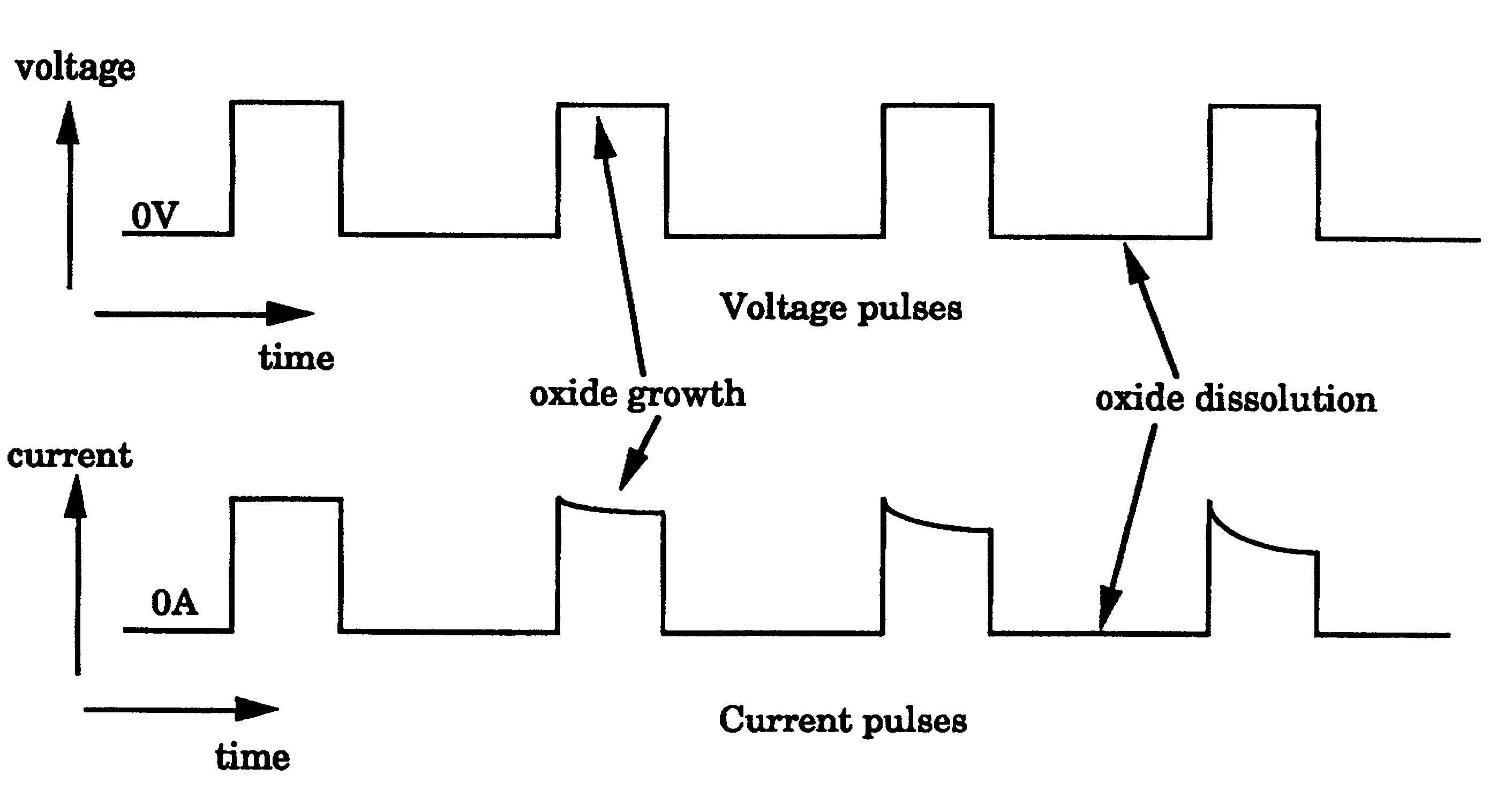
A laser wafer sketched in FIG. 12 was processed by the method of this invention to form a 120 nm thick oxide layer with a resultant ridge height of 86 mm. The oxide was found to be unstable when exposed to ambient air for several hours. There was no "travelling oxide" because the GWA solution did not etch the oxide when the pulse was off. We discovered that we could make a stable oxide, however, by reversing the polarity of the pulses. In the reversed current mode, the oxide etched and we could make a ridge 200 nm high, with a 120 nm thick oxide layer terminating in the AlInP cladding layer using a cycle of three polarity flips. In a production mode, the positive voltage pulse could be followed by a negative pulse to both grow and dissolve the oxide at a constant rate. In fact, a thin oxide could be used at the beginning of the process which would grow the oxide faster, and the etching of the oxide could be controlled by the reversed curren...


PUM

PropertyMeasurementUnit
current densityaaaaaaaaaa
etch rateaaaaaaaaaa

Abstract

A multilayer compound semiconductor is contacted with an electrically conducting fluid, and a current is passed between the semiconductor and the fluid. The current passes is monitored, and the current is controlled in response to the monitoring.

Description

The field of the invention is the field of semiconductor processing, and in particular to the field of multilayer compound semiconductor processing.The background of the invention is given in great detail in the above identified applications.A schematic drawing of the prior art fabrication procedure for a monolithic array of semiconductor laser diodes is shown in FIG. 1. A substrate 2 of n-type GaAs material has a number of layers grown epitaxially. The important cladding layers 6 of n-type AlGaAs and 7 of p-type AlGaAs surround an active layer 4 which normally has a lower bandgap than the cladding layers and may be composed of many layers of AlGaAs, GaAs, InGaAs, or other III-V semiconductor compounds. A layer of exposed and developed photoresist 8 is shown with openings 9 etched in the photoresist. Step b of the prior art procedure uses an etching step to etch vee grooves in the cladding layer 7, generally through the active layer 4 and into the other cladding layer 6. A blanket l...

Claims


Application Information

Patent Timeline
Patent Type & Authority Patents(United States)
IPC IPC(8): C25D11/02C25D11/32H01L21/465H01L21/471H01L21/02H01L21/316H01L21/3063
CPCC25D11/32H01L21/02178H01L21/02233H01L21/02241H01L21/02258H01L21/30635H01L21/31666H01L21/465H01L21/471
Inventor ZORY, JR., PETER S.
Owner ZORY JR PETER S
Why Eureka
Try Eureka