Method of molding plastic semiconductor packages

a technology of semiconductor packaging and plastic body, which is applied in the field of semiconductor packaging, can solve the problems of molding compound to adhere, small and fragile, and large amount of heat generation

Inactive Publication Date: 2001-10-30
AMKOR TECH SINGAPORE HLDG PTE LTD
View PDF8 Cites 75 Cited by
  • Summary
  • Abstract
  • Description
  • Claims
  • Application Information

AI Technical Summary

Problems solved by technology

The dies are relatively small and fragile, are susceptible to harmful environmental elements, particularly moisture, and generate a relatively large amount of heat in a relatively small volume during operation.
A problem with the conventional package transfer molding technique relates to the tendency of the molding compound to adhere to the surfaces of the molding tool, including the cavity, chase and ejector pins of the mold, that come into contact with the plastic molding compound during the molding process.
If the molding compound adheres appreciably to these surfaces of the mold, the package will not release completely from the mold, resulting in the formation of cracks or craters in the package body, defective packages, and/or the subsequent penetration of the package by damaging moisture.
Another, countervailing, package molding problem relates to an incomplete or defective adhesion of the plastic package body to the package components, i.e., the leadframe or substrate, wire bonds, the die, and other components.
This can result in a delamination of the plastic body from the components and the subsequent propagation of cracks and penetration of the package by moisture.
In particular, where delamination occurs at a boundary of the package body, a microscopic crack is created for the penetration of the package by mois...

Method used


Image

  • Method of molding plastic semiconductor packages
  • Method of molding plastic semiconductor packages
  • Method of molding plastic semiconductor packages

Examples


Embodiment Construction

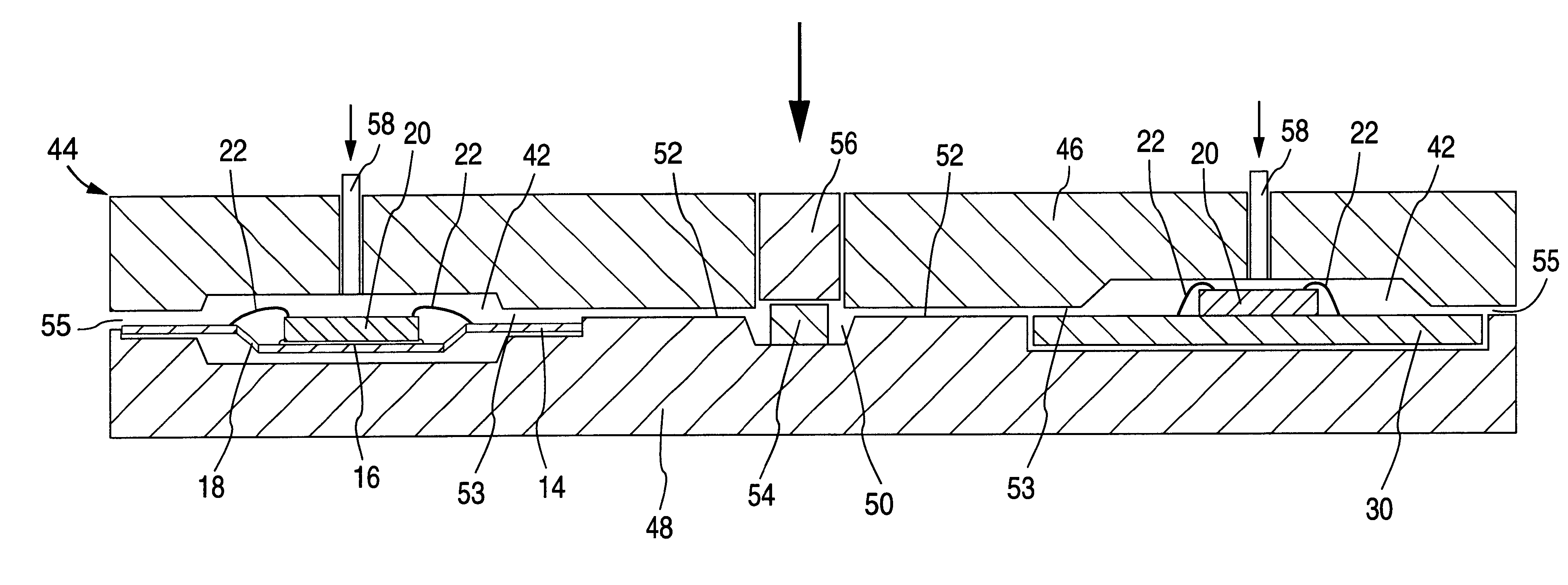
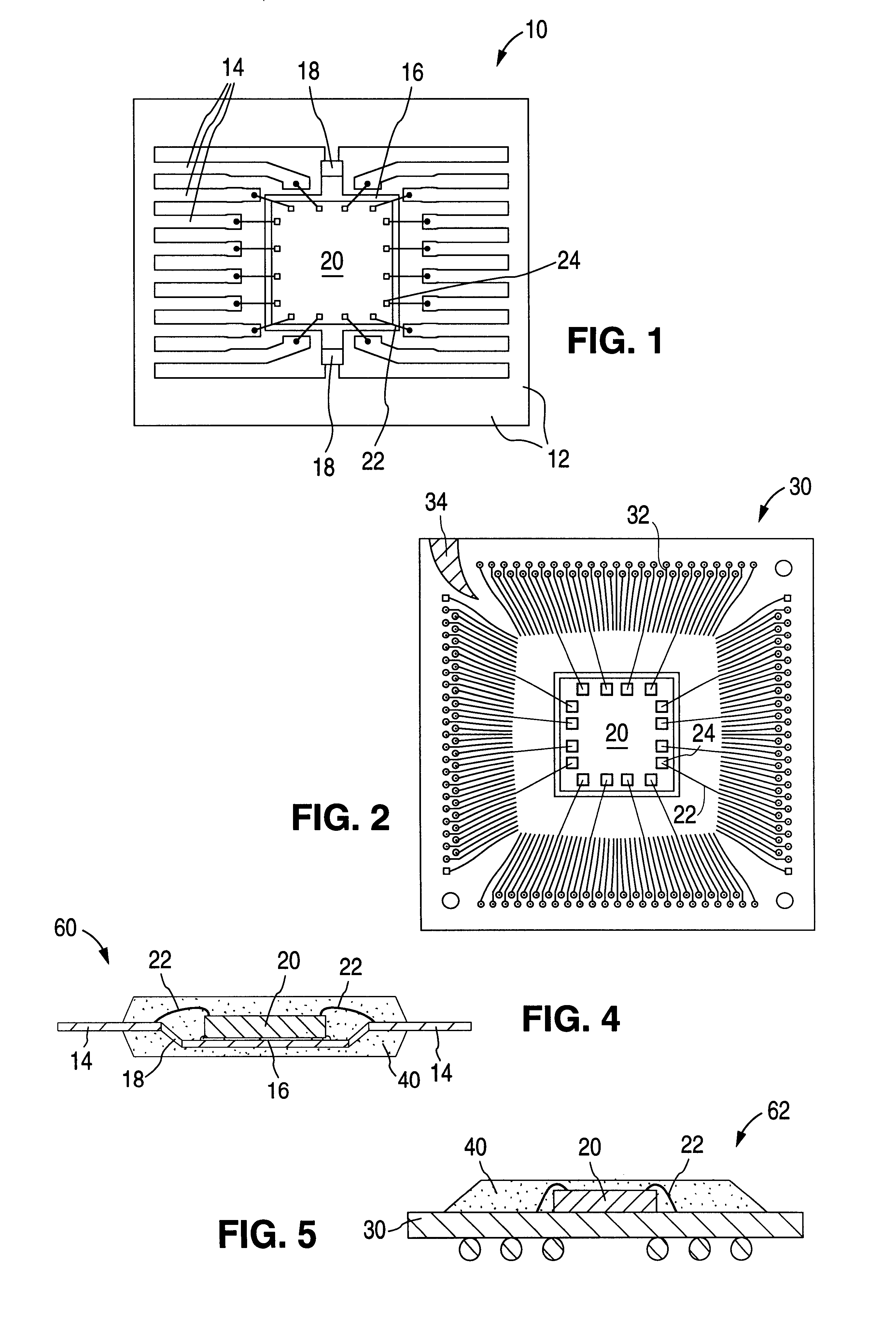
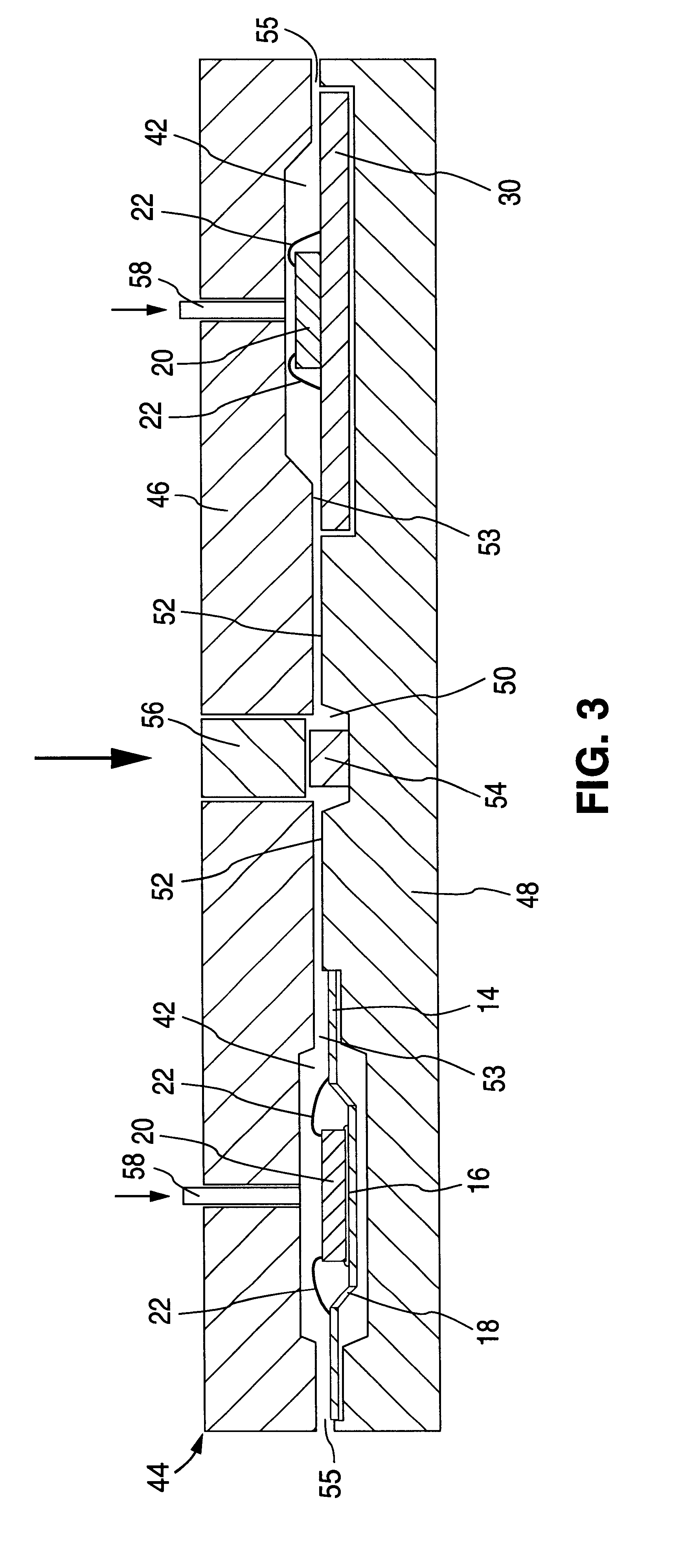
FIGS. 1, 3 and 4 show the sequential stages in the manufacture of a typical leadframe type of semiconductor package, while FIGS. 2, 3 and 5 show similar stages in the manufacture of a typical grid array package.

In FIG. 1, a top plan view of a leadframe 10 is shown. The metal lead-frame 10 comprises a rectangular frame 12 having a central region and a matrix of leads 14 extending from it inwardly toward the central region. A die mounting pad 16 is supported in the central region of the frame by two or more tie-bars 18. A semiconductor die 20 is mounted by an adhesive to the upper surface of the die mounting pad 16 and is electrically connected to selected ones of the inner portions of the leads 14 by a plurality of fine, conductive bonding wires 22 that are bonded at their opposite ends to pads 24 on the die and selected ones of the leads 14, respectively.

A top plan view of a substrate 30 used in the manufacture of a typical grid array package is shown in FIG. 2. The substrate 30 com...


PUM

PropertyMeasurementUnit
Thicknessaaaaaaaaaa
Electrical resistanceaaaaaaaaaa
Adhesion strengthaaaaaaaaaa

Abstract

In the manufacture of semiconductor packages having molded plastic bodies, the plating of all of the surfaces of the molding tool that comes into contact with the molten resin during molding with a nodular thin dense chromium ("NTDC") coating prevents the surfaces from adhering to the package body and ensures good package release, without formation of cracks or craters in the package body. This, in turn, permits the amount of both release agents and adhesion promoters used in the molding compound to be substantially reduced, or eliminated altogether, thereby resulting in a package body having improved strength and adhesion with the components of the package, and hence, an improved resistance of the package body to the propagation of cracks and its subsequent penetration by moisture.

Description

1. Field of the InventionThis invention pertains to semiconductor packaging in general, and in particular, to an improved method for molding the plastic bodies of semiconductor packages.2. Description of the Related ArtIntegrated circuits ("ICs") are formed on a single die, or "chip," cut from a semiconductor wafer containing a large number of identical dies. The dies are relatively small and fragile, are susceptible to harmful environmental elements, particularly moisture, and generate a relatively large amount of heat in a relatively small volume during operation. Accordingly, ICs must be packaged in affordable, yet robust, packages that protect them from the environment, permit them to be reliably mounted to and interconnected with, for example, a printed circuit board ("PCB") populated with associated electronic components, and to dissipate effectively the heat they generate during operation.In both leadframe and grid array types of packages, a leadframe or substrate assembly ha...

Claims


Application Information

Patent Timeline
IPC IPC(8): B29C45/37B29C45/40B29C45/14H01L21/02H01L21/56
CPCB29C45/14655B29C45/37H01L24/97H01L21/565B29C45/401H01L2224/97H01L2224/73265H01L2224/49171H01L2224/48247H01L2224/48227H01L2224/32245H01L2924/15311H01L2924/01079H01L2924/01078H01L2924/01046H01L2924/01012H01L2224/48091H01L2924/00014H01L2924/00H01L2924/181H01L2924/14H01L2924/00012
Inventor CROWLEY, SEAN T.CHENEY, GERALD L.RAZU, DAVID S.
Owner AMKOR TECH SINGAPORE HLDG PTE LTD
Why Eureka
Try Eureka