
Method for making silicon nitride-oxide ultra-thin gate insulating layers for submicrometer field effect transistors

a field effect transistor and ultra-thin technology, applied in the field of integrated circuit device manufacturing, can solve the problems of unstable electrical characteristics of the fet device, unacceptable standby power of the fet,

Inactive Publication Date: 2001-11-27
TAIWAN SEMICON MFG CO LTD
View PDF11 Cites 39 Cited by
  • Summary
  • Abstract
  • Description
  • Claims
  • Application Information

AI Technical Summary

Benefits of technology

It is another object of this invention to form this ultra-thin nitride-oxide gate insulating layer using a novel low-pressure rapid thermal process and an ultra-thin silicon nitride layer that also reduces or prevents boron penetration.
In accordance with the above objects, a method for fabricating improved ultra-thin gate oxides for deep sub-micrometer FETs having channel lengths of less than 0.18 micrometers (.mu.m) is provided. The method results in a very controllable ultra-thin silicon nitride-oxide gate insulating layer (about 18 to 30 Angstroms thick) that also reduces the gate oxide leakage currents and boron penetration. The method also provides a means of forming a very controllable interface silicon oxide layer at the substrate surface while providing a nitrogen-rich oxidized silicon nitride layer. The method for forming this improved FET nitride-oxide gate insulating layer begins by providing a semiconductor substrate consisting of single-crystal silicon and having device areas that are typically surrounded and electrically isolated by field oxide areas. A thin silicon nitride layer is grown on the substrate surface in the device areas. The silicon nitride layer is formed in a low-pressure rapid thermal process (RTP) by applying a first heating step while subjecting the substrate to a first gas ambient containing nitrogen, such as ammonia (NH.sub.3), while insuring that the RTP chamber is free of oxygen. The silicon nitride layer is then subjected to a oxidation second heating step and a second gas ambient containing nitrogen and oxygen. The second gas ambient is preferably dinitrogen oxide (N.sub.2 O), and the second heating step is at a sufficiently high temperature to form a silicon oxide (SiO.sub.2) layer at the interface between the silicon nitride layer and the substrate an the device areas. Concurrently the oxidation is carried out in the nitrogen-rich gas (N.sub.2 O) to retain a high nitrogen concentration in the oxidized silicon nitride layer This results in an ultra-thin nitrogen-rich silicon nitride-oxide gate insulating layer (about 18 to 30 Angstroms thick) that achieves the above objectives.

Problems solved by technology

However, as the FETs are down scaled to submicrometer channel length, the FET device experiences a number of undesirable electrical characteristics results.
When this oxide leakage current becomes comparable to the FET off-current (I.sub.off), the standby power for the FET becomes unacceptably high.
This nitrogen-enriched layer 12 further reduces the boron penetration that can otherwise occur during subsequent processing, resulting in unstable electrical characteristics of the FET device.

Method used


Image

  • Method for making silicon nitride-oxide ultra-thin gate insulating layers for submicrometer field effect transistors
  • Method for making silicon nitride-oxide ultra-thin gate insulating layers for submicrometer field effect transistors
  • Method for making silicon nitride-oxide ultra-thin gate insulating layers for submicrometer field effect transistors

Examples


Embodiment Construction

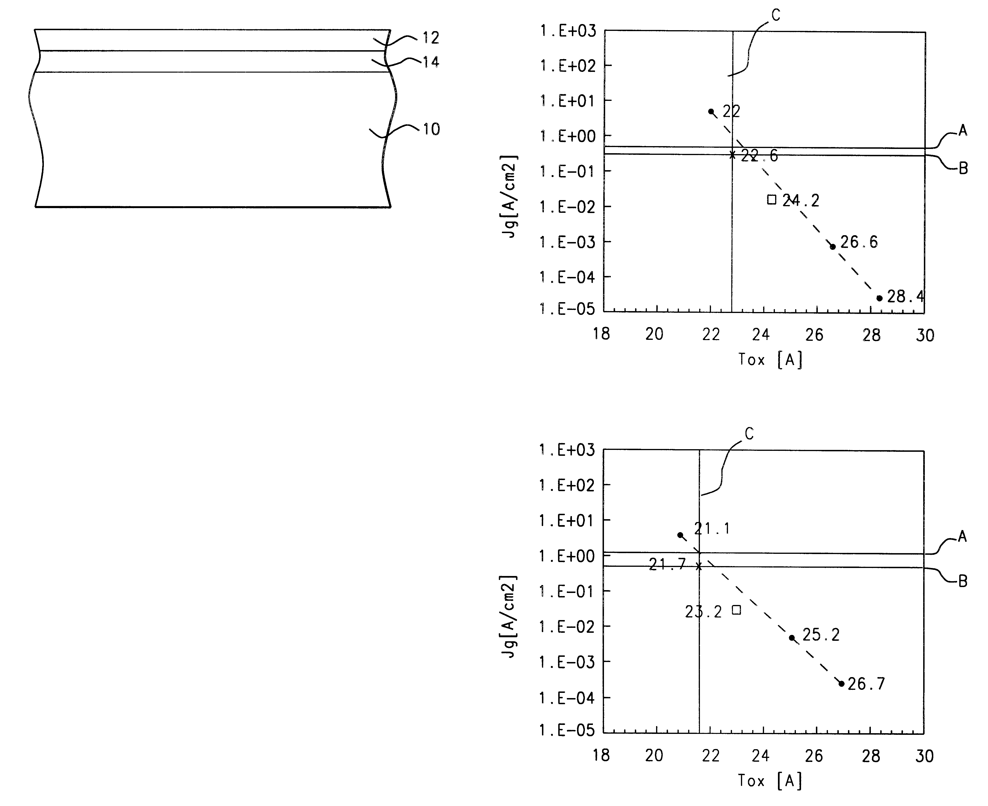
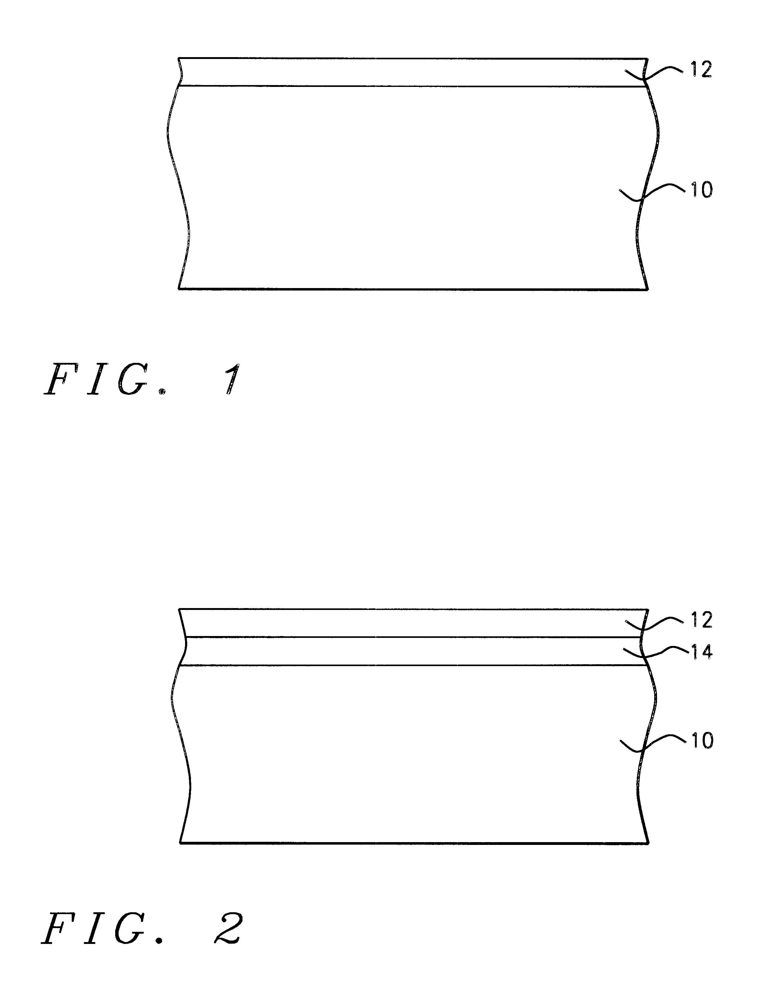
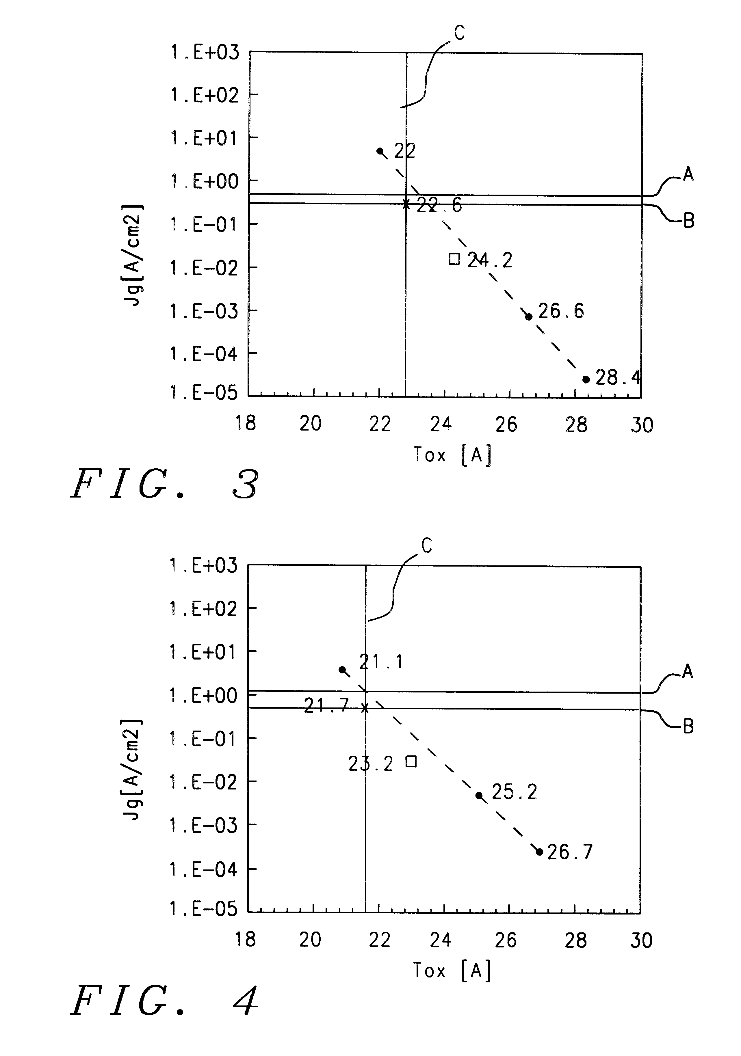
To better appreciate the advantages of this novel process for making ultra-thin FET gate insulating layers, test structures were fabricated and the nitride-oxide gate oxide leakage currents were measured as a function of gate oxide thickness. The results were then compared with the more conventional ISSG process using nitrous oxide (NO) as the oxidation gas. The graph in FIG. 3 is for a gate oxide grown on an N-doped substrate (or wafer), and the graph in FIG. 4 is for a gate oxide grown on a P-doped substrate. The vertical axis in each graph is the leakage current density J.sub.g measured on a log scale in Ampere per square cm (A / cm.sup.2), and the horizontal axis is the gate oxide thickness T.sub.ox measured in Angstroms. After forming the ultra-thin silicon nitride-oxide gate insulating layer (layers 12 and 14), an N-doped polysilicon gate electrode was formed over an oxide area of 1.0 E .sup.- 4 cm.sup.2. The current density was measured using a model HP4284 instrument manufactu...


PUM


Abstract

A method for making an improved ultra-thin silicon nitride-oxide gate insulating layer for field effect transistors (FETs) is achieved. After forming a field oxide to electrically isolate device areas on a silicon substrate, an ultra-thin silicon nitride-oxide insulating layer is formed in two process steps. In the first process step a silicon nitride layer is formed on the device areas on the substrate using a low-pressure rapid thermal process (LP-RTP) and a reactant gas of ammonia (NH3) while insuring that the RTP tool is free of oxygen. Then a second process step is carried out sequentially in the same LP-RTP at an elevated temperature and using an oxygen-rich ambient (dinitrogen oxide N2O) as a reoxidation gas. The non-self-limiting characteristic of the ultra-thin-silicon nitride layer results in the controllable diffusion of the dissociated oxygen (O) and nitrous oxide (NO) through the silicon nitride layer to form a thin good quality silicon oxide layer on and in the substrate surface.

Description

(1) Field of the InventionThe present invention relates to the fabrication of integrated circuit devices on semiconductor substrates, and more particularly relates to a method for making an improved ultra-thin silicon nitride-oxide gate insulating layer for field effect transistors with deep submicrometer channel lengths.(2) Description of the Prior ArtAdvances in the semiconductor process technologies in the past few years have dramatically decreased the device feature sizes and increased circuit density on integrated circuit chips. The device used the most for these Ultra Large Scale Integration (ULSI) applications is the Field Effect Transistor (FET) which consists of a polysilicon or polycide gate electrode formed over a thin gate oxide with self-aligned source / drain contact areas. The popular choice of FETs is because of their very small size, high packing density, low power consumption, high yields, and low cost of manufacturing.The conventional FETs are typically fabricated b...

Claims


Application Information

Patent Timeline
IPC IPC(8): H01L21/28H01L21/02H01L21/314H01L21/318H01L29/51
CPCH01L21/28202H01L21/3144H01L21/3185H01L29/513H01L29/518H01L21/02164H01L21/0214H01L21/02255H01L21/022H01L21/02326H01L21/02247H01L21/02337
Inventor YU, MO-CHIUN
Owner TAIWAN SEMICON MFG CO LTD
Learn More