Thin film circuit with improved carrier mobility

a thin film transistor and carrier mobility technology, applied in the field of semiconductor circuits, can solve the problems of difficult in practice to form an operational amplifier circuit using such thin film transistors, and achieve the difficulty of forming a thin gate insulation film, technically and economically difficult to achiev

Inactive Publication Date: 2001-12-18
SEMICON ENERGY LAB CO LTD
View PDF15 Cites 39 Cited by
  • Summary
  • Abstract
  • Description
  • Claims
  • Application Information

AI Technical Summary

Problems solved by technology

In practice, since it is difficult to provide two transistors having completely identical characteristics, efforts are being made toward manufacturing techniques to provide transistors that are as similar to each other as possible in their characteristics.
For this reason, it has been di

Method used


Image

  • Thin film circuit with improved carrier mobility
  • Thin film circuit with improved carrier mobility
  • Thin film circuit with improved carrier mobility

Examples


Embodiment Construction

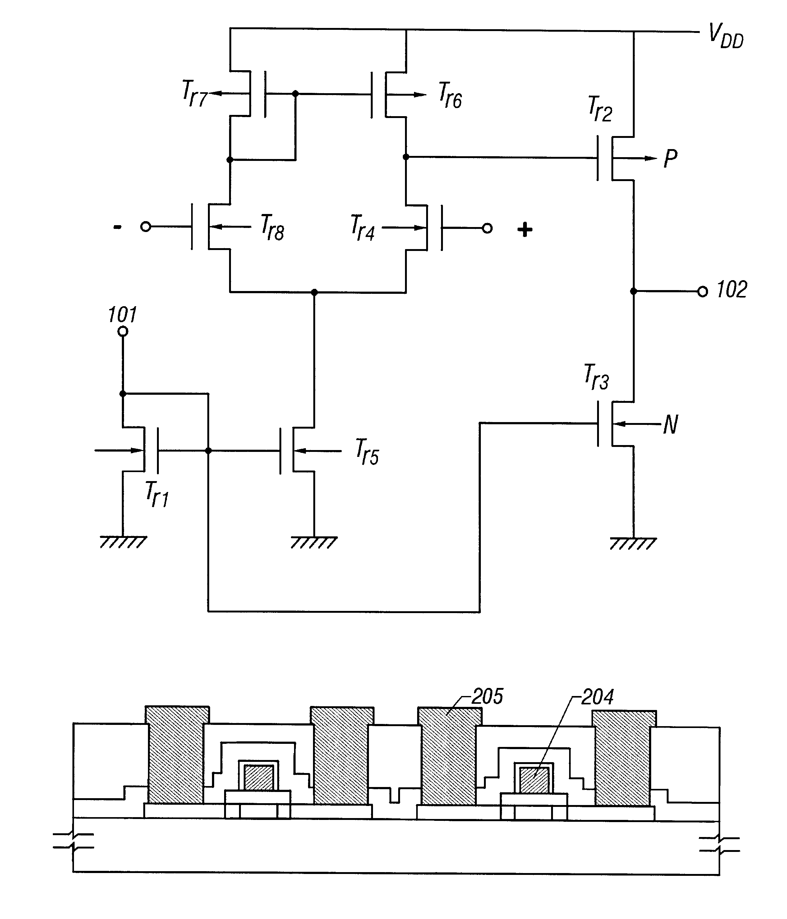
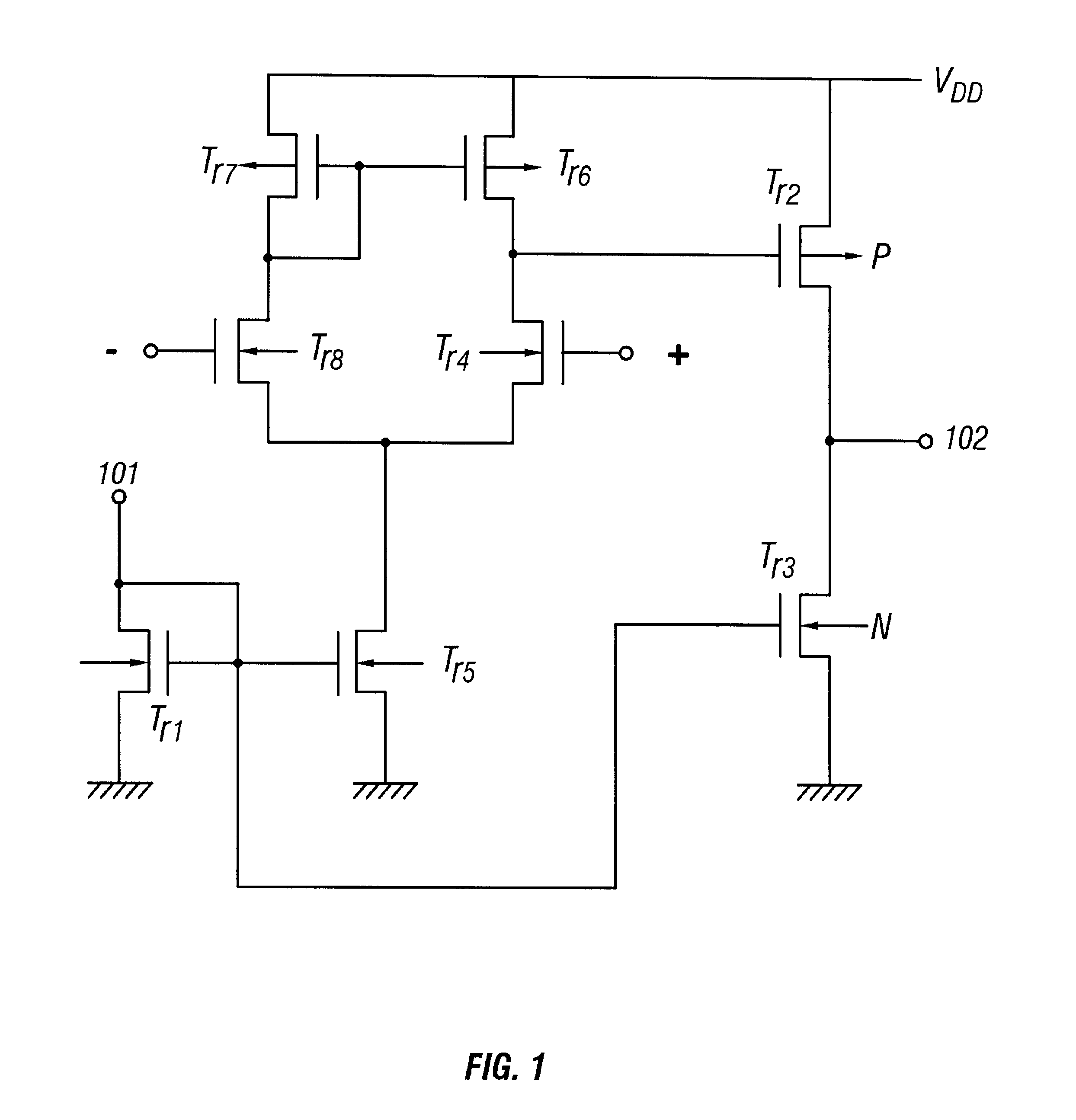
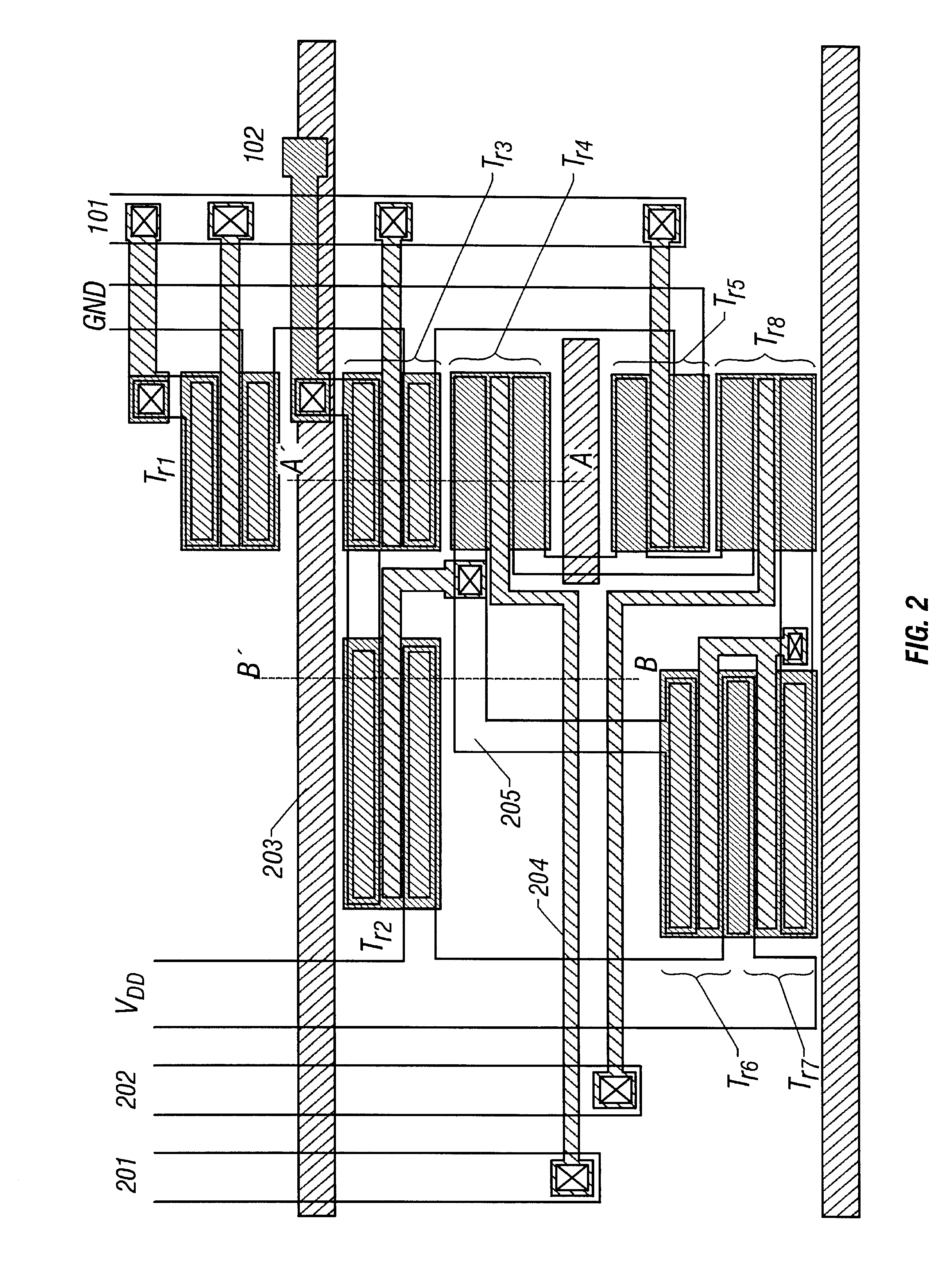
An active layer is formed by a crystalline silicon film having a structure with a multiplicity of crystal structures extending in a certain direction arranged in parallel. The direction in which the crystal structures extend is aligned with the direction of the moving direction of carriers. This makes it possible to obtain advantages that can not be achieved by conventional devices utilizing single crystal semiconductors and polycrystalline semiconductors.

The short channel effect is less likely to occur on such a crystalline silicon film formed by a multiplicity of crystal structures extending in the form of columns in a certain direction even if the dimension of a channel is reduced because the movement of carriers is regulated in the direction in which they extend.

The reason is based on the presence of a multiplicity of elongate and substantially monocrystalline regions (columnar regions) extending in parallel in the channel region. These suppress the expansion of a depletion laye...


PUM


Abstract

A practical operational amplifier circuit is formed using thin film transistors.An operational amplifier circuit is formed by thin film transistors formed on a quartz substrate wherein 90% or more of n-channel type thin film transistors have mobility at a value of 260 cm2/Vs or more and wherein 90% or more of p-channel type thin film transistors have mobility at a value of 150 cm2/Vs or more. The thin film transistors have active layers formed using a crystalline silicon film fabricated using a metal element that promoted crystallization of silicon. The crystalline silicon film is a collection of a multiplicity of elongate crystal structures extending in a certain direction, and the above-described characteristics can be achieved by matching the extending direction and the moving direction of carriers.

Description

1. Field of the InventionThe present invention relates to a semiconductor circuit utilizing a crystalline silicon film formed on a quartz substrate or the like and, more particularly, to a semiconductor circuit having the function of an operational amplifier.2. Description of the Related ArtRecently, research is being carried out on techniques for forming semiconductor devices utilizing a crystalline silicon film on a quartz substrate in an integrated manner. A typical example of such techniques is a technique for providing an active matrix circuit and a peripheral driving circuit for driving the same circuit on a single quartz substrate or glass substrate.The required circuit configurations include active matrix circuits, shift register circuits and buffer circuits.An active layer of a thin film transistor forming a part of a circuit is formed using a crystalline silicon film. A crystalline silicon film can be fabricated by forming an amorphous silicon film on a substrate and then ...

Claims


Application Information

Patent Timeline
IPC IPC(8): H01L29/66H01L21/70H01L21/336H01L21/02H01L29/786H01L27/12H01L21/84G02F1/136G02F1/1368H01L21/77H01L29/04
CPCH01L27/12H01L29/04H01L29/66757H01L29/78621H01L29/78675H01L27/1277H01L21/02532H01L21/02672
Inventor YAMAZAKI, SHUNPEIKOYAMA, JUNOHTANI, HISASHI
Owner SEMICON ENERGY LAB CO LTD
Why Eureka
Try Eureka