Electro-optical transceiver system with controlled lateral leakage and method of making it

a transceiver and optical technology, applied in the direction of lasers, semiconductor laser structural details, semiconductor lasers, etc., can solve the problems of data transfer into and out of processors, light leakage laterally, and noise in the received signal

Inactive Publication Date: 2002-02-05
ALTERA CORP
View PDF12 Cites 81 Cited by
  • Summary
  • Abstract
  • Description
  • Claims
  • Application Information

AI Technical Summary

Problems solved by technology

However, data transfer into and out of processors remains a limiting factor.
However, some light leaks laterally, and it can be detected by a nearby detector.
This light adds noise to the signal received at that detector, which detracts from the overall performance of the system.
In many devices, there is a need to ma...

Method used


Image

  • Electro-optical transceiver system with controlled lateral leakage and method of making it
  • Electro-optical transceiver system with controlled lateral leakage and method of making it
  • Electro-optical transceiver system with controlled lateral leakage and method of making it

Examples


Embodiment Construction

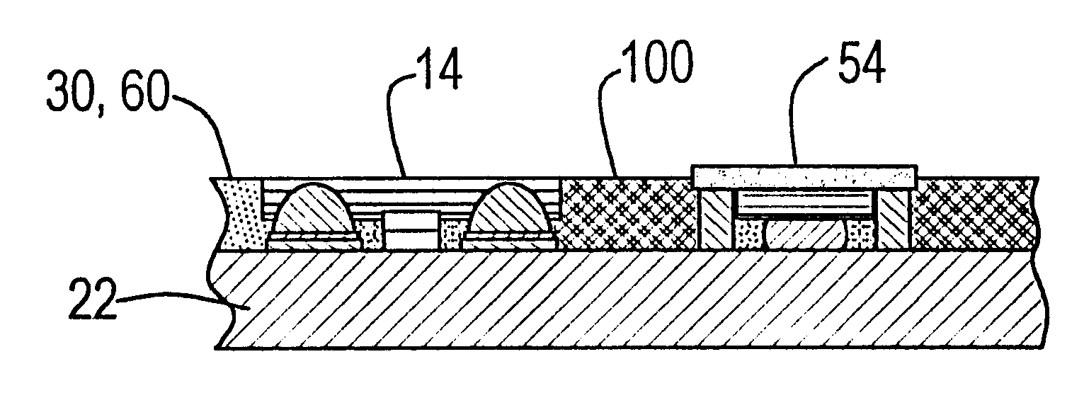
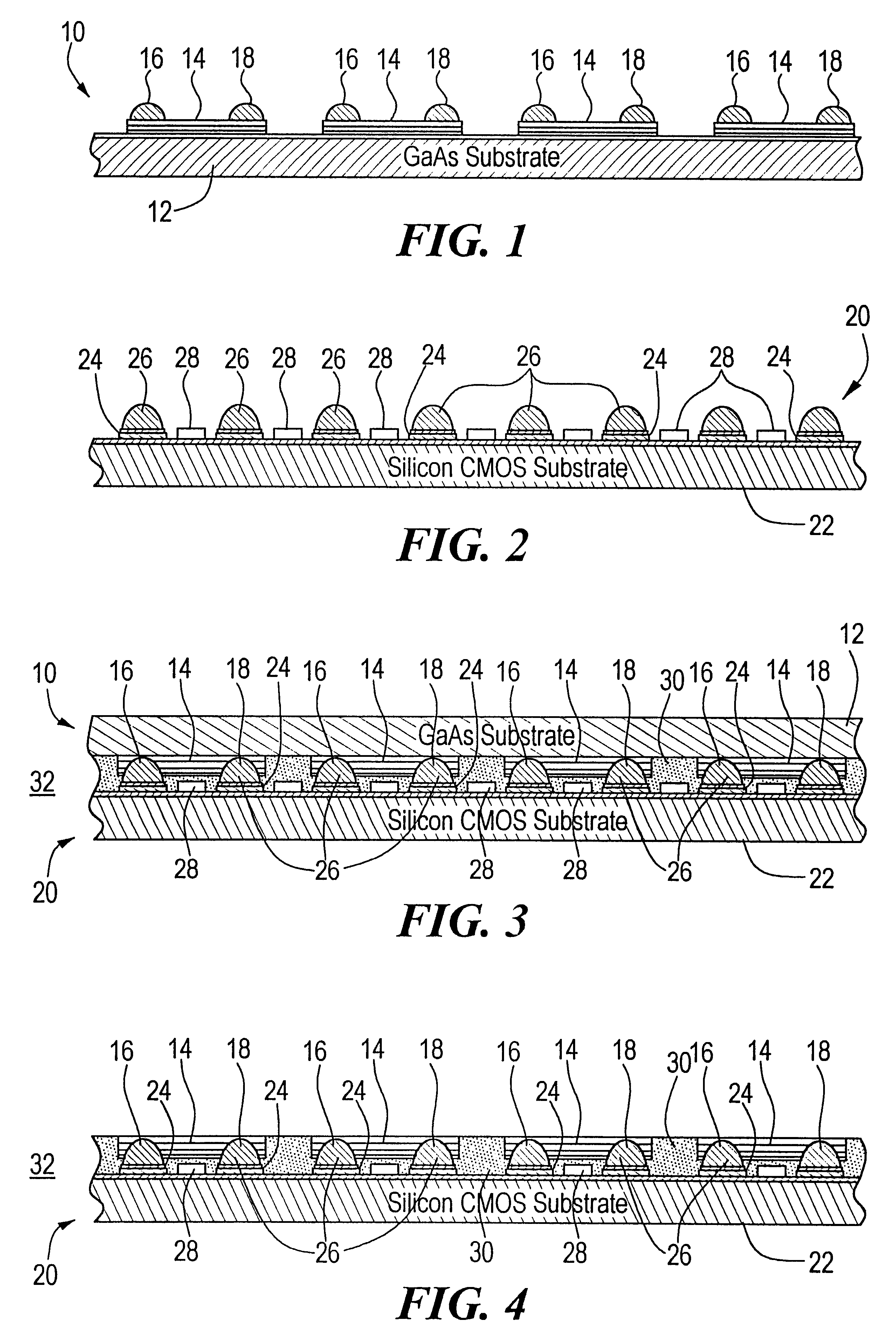
There is shown in FIG. 1 a first chip 10 including a GaAs substrate 12 having grown on it a number of vertical cavity surface emitting laser (VCSEL) emitters 14. Mounted on each of the VCSELs 14 are a number of solder balls or bumps two of which are shown 16 and 18. Some of these devices 14 are actually dummy devices and will be removed as seen subsequently with respect to FIGS. 5 and 6.

The second chip 20, FIG. 2, includes a silicon CMOS substrate 22 which carries a number of metal landing pads 24 each containing a solder ball or bump 26 so arranged that they mate with the solder bumps 16 and 18 of chip 10, FIG. 1. Also shown on chip 20 are portions 28 of an electronic circuit in this case an application specific integrated circuit (ASIC).

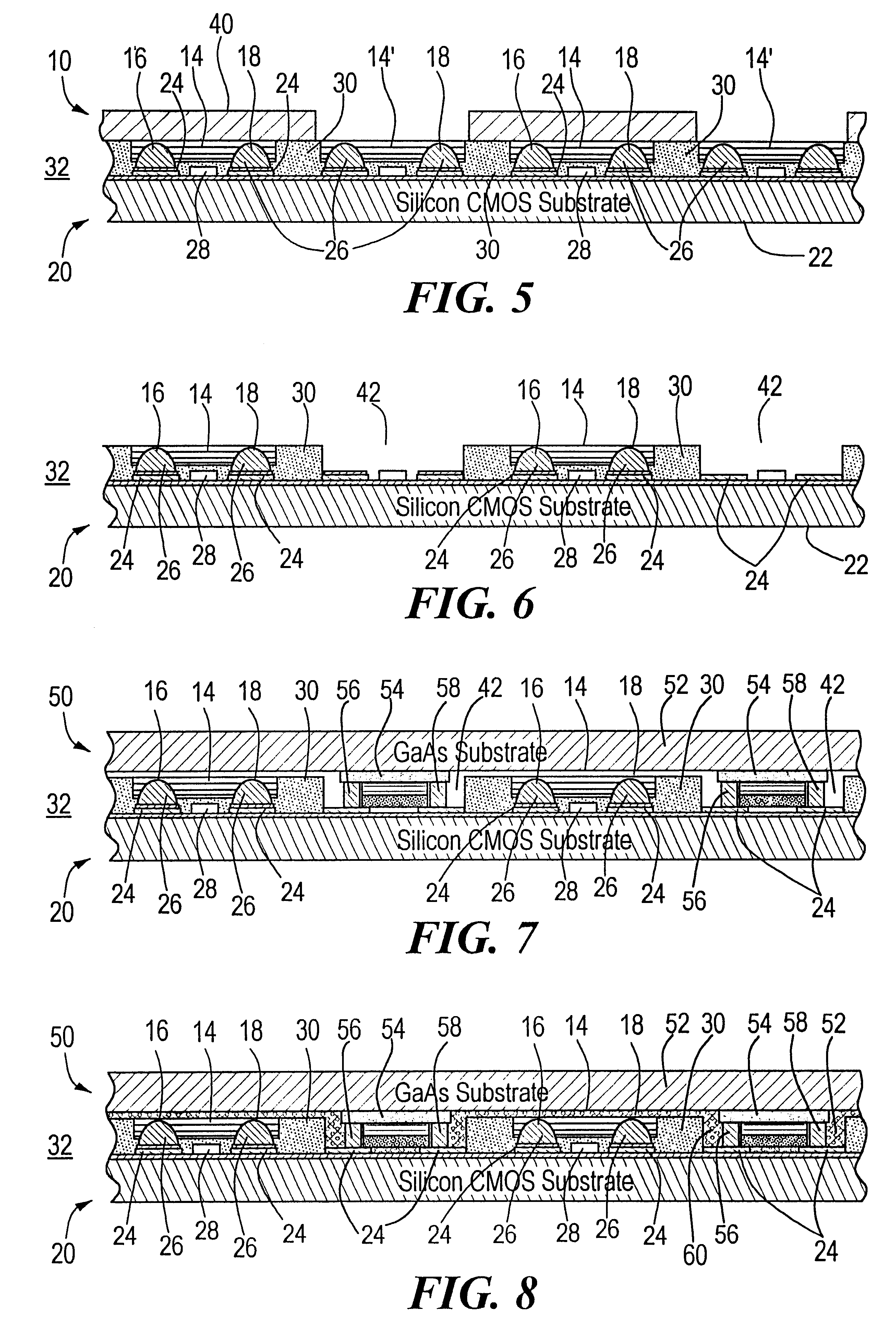
The first chip 10, FIG. 1 is flip-chipped and bump bonded onto the second chip 20 as shown in FIG. 3 and filled with an underfill 30 such as an epoxy, a photoresist, or any other suitable flowable hardener. Underfill 30, FIG. 3, fills the voids bet...


PUM


Abstract

An electro-optical transceiver system with controlled lateral light leakage and a method of making such a system includes a plurality of emitter devices and detector devices including at least one of each, arranged in a planar array for transmitting and receiving, respectively, energy in a predetermined wavelength and a blocking medium disposed interstitially of the devices and being absorbing at the predetermined wavelength for blocking energy at the predetermined wavelength laterally leaking from an emitter device to one or more detector devices.

Description

This invention relates to an electro-optical transceiver system with controlled lateral leakage and a method of making it.BACKGROUND OF INVENTIONComputers and related peripheral equipment, satellite and communication systems are becoming ever more sophisticated and powerful. However, data transfer into and out of processors remains a limiting factor. The combination of increased parallelism and optics is the focus of optical interconnect technology. One approach to optical interconnect technology uses so-called flip-chip techniques where the advantages of silicon process technology are combined with the optical properties of III-V semiconductor materials. In this technology, emitter-detector arrays are fabricated separately from a CMOS substrate. The emitter-detector arrays are then inverted, aligned with the CMOS substrates and secured in place using solder balls to form electrical contacts and epoxy to rigidly mount the emitter-detector array to the CMOS chip. In one construction ...

Claims


Application Information

Patent Timeline
IPC IPC(8): H01L25/075H01S5/00H01S5/026H01S5/183H01S5/02
CPCH01L25/0753H01S5/0262H01S5/021H01S5/0217H01S5/423H01S5/0264H01S5/183H01S5/02272H01L2924/0002H01S5/0237H01L2924/00
Inventor TREZZA, JOHN A.DUDOFF, GREGORY K.
Owner ALTERA CORP
Why Eureka
Try Eureka